Physical vapor deposition method (PVD) is a vacuum coating process that deposits thin, hard films—often 1–5 microns—onto metal or polymer substrates. It uses a physical source of material (like a metal target) that vaporizes and condenses on parts. For Woodbridge manufacturers, PVD improves wear resistance, cuts friction, and extends tool life in high-throughput production.
By Ron — Sputtek • Last updated: 2026-07-05
Overview and why this guide
This guide explains the physical vapor deposition method in plain, practical terms. You’ll learn what PVD is, why it matters, how it works, the main process types, best practices for design and production, essential tools, and real examples from Sputtek’s Woodbridge facility.
PVD is central to modern surface engineering. In our experience, shops that adopt it report measurable gains: longer mean-time-between-failure (MTBF), steadier throughput, and more predictable quality audits. Thin films 1–5 μm can raise surface hardness into the ~1,800–3,500 HV range, while many DLC variants deliver coefficients of friction near 0.1–0.2 under dry sliding.
- What you’ll get here:
- Clear definitions for engineers, QA leads, and toolmakers
- Side-by-side comparisons of sputter, arc, e-beam, and HiPIMS
- Actionable design-for-coating rules with tolerances and geometry tips
- Production playbooks for prototyping through volume batches
- Case snapshots from stamping, molds, cutting tools, and components

What is the physical vapor deposition method?
The physical vapor deposition method (PVD) is a set of vacuum processes—like sputtering and arc evaporation—that physically vaporize a source material and condense it as a thin, adherent coating on parts. Typical films measure 1–5 μm, add 1–3 μm per side, and boost wear resistance without distorting tight tolerances.
In PVD, the chamber operates under high vacuum—often below 1×10⁻³ mbar—to minimize contamination and enable line-of-sight deposition. Substrates are heated (commonly 200–500 °C depending on material) and biased to promote adhesion. Film chemistries include TiN, TiCN, AlTiN, CrN, ZrN, and DLC, each tuned for a specific tribological regime.
- Core outcomes engineers care about:
- Wear resistance: Surface hardness in the 1,800–3,500 HV band limits abrasive and adhesive wear.
- Lower friction: DLC and MoS2-like stacks often cut μ down to ~0.1–0.2.
- Thermal stability: AlTiN-class films maintain hardness well beyond 800 °F in dry cutting.
- Thin, conformal layers: Typical build adds microns, not millimeters—critical for molds and dies.
As Canada’s largest PVD/DLC service provider, Sputtek runs multiple systems that support prototyping and high-volume production in our modern Woodbridge facility. Our in-house prep (degreasing, blasting, polishing) and after-coating lapping close the loop for consistent quality cycles.
Why PVD matters for manufacturers
PVD increases uptime, stabilizes part quality, and extends maintenance intervals by improving surface hardness, lubricity, and corrosion resistance. Manufacturers see fewer unplanned stoppages, better dimensional stability, and more predictable tool life—especially in stamping, molding, machining, and die casting.
Here’s the thing: most scrap and downtime come from surfaces failing early. At line rates measured in parts-per-minute, one sticky cavity or a galling die corner can ripple through OEE. We’ve found that moving to the physical vapor deposition method turns recurring micro-failures into rare events you can plan around.
- Stamping dies: With CrN or AlTiCrN, edge pickup and galling drop noticeably; many shops stretch regrind windows.
- Molding tools: DLC reduces release force; in packaging, cavities eject more cleanly at cycle times under 3 s.
- Cutting tools: AlTiN/AlCrN sustain speed; tool life often rises from dozens to hundreds of minutes per edge.
- Components: For high-contact assemblies, μ reduction and corrosion resistance stabilize duty cycles.
In regulated sectors (medical, pharma, nuclear), paper trails and repeatability matter as much as performance. Sputtek’s ISO 9001:2015 system and Nuclear N299.3 vendor approval support audits, traceability, and change control—an operational safeguard alongside the coating itself.
How the PVD process works (step-by-step)
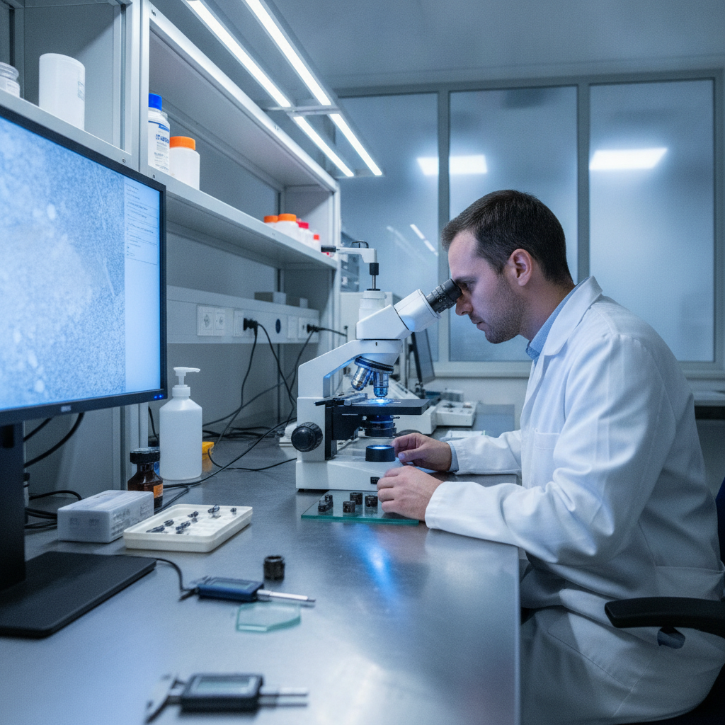
PVD converts solid material to a vapor in vacuum, then condenses it as a dense, adherent film on biased, heated parts. The workflow spans cleaning, surface activation, deposition (sputter/arc/e-beam/HiPIMS), controlled cooling, and post-finishing—each step verified by in-process gauges and QC checks.
- Pre-cleaning and prep (degreasing, ultrasonic, microblasting). Residual oils at parts-per-million can seed pinholes; we target clean surfaces verified by contact-angle and gravimetric checks.
- Fixturing. Rotary racks and planetary fixtures even out film thickness; we design to ±0.5–1.0 μm targets where needed.
- Vacuum and heat. Pumpdown to ~1×10⁻³ mbar or better; substrate temp matched to metallurgy and temper limits.
- Surface activation. Argon sputter etch and biasing raise adhesion energy; partial pressure typically 10−2–10−1 mbar.
- Deposition. Rate ranges from tenths to a few μm/hour depending on method and chemistry.
- Cooldown and unload. Controlled cooling prevents condensation staining and thermal shock on polished surfaces.
- Post-processing. Lapping/polishing optimize Ra and Rz; we see Ra reductions into sub-0.05 μm on mirror features.
Our guide to PVD systems explains how chamber geometry and cathode layout affect uniformity. For Woodbridge production teams, repeatable racks and validated prep steps are the fastest path to first-pass yield at scale.
Types of PVD methods (and when to use them)
The main PVD processes are sputtering (DC/RF), cathodic arc evaporation, electron-beam evaporation, and HiPIMS. Choose based on density, stress, step coverage, droplet tolerance, and temperature limits. Sputtering yields smooth films; arc is fast and dense; e-beam supports high-rate evaporation; HiPIMS improves ionization and adhesion.
Sputtering (DC, RF, magnetron)
- Best for: Smooth, low-droplet films, multilayers, and nitrides/carbides on tight-tolerance molds.
- Deposition rate: Moderate; typical 0.5–2 μm/hr depending on target power and pressure.
- Notes: Excellent control of stress and stoichiometry; great for optical-grade finishes and DLC underlayers.
Cathodic arc evaporation
- Best for: Ultra-dense films that shrug off abrasion on dies and cutting tools.
- Deposition rate: High; often 2–5 μm/hr with right cathode current.
- Notes: May introduce droplets; post-polishing or filtration mitigates. Adhesion is excellent with proper bias.
Electron-beam evaporation
- Best for: High-rate evaporation of metals and some ceramics; line-of-sight applications.
- Deposition rate: High; multi-μm/hr possible with large melt pools.
- Notes: Superb for decorative or functional metal layers; step coverage is more directional than sputter.
HiPIMS (High-Power Impulse Magnetron Sputtering)
- Best for: Tough adhesion and dense structure without arc droplets.
- Deposition rate: Lower than DC magnetron, but with improved ionization for tight interfaces.
- Notes: Great for advanced multilayers and diffusion barriers on complex geometries.
| Process | Film Density | Surface Smoothness | Typical Rate | Best Uses |
|---|---|---|---|---|
| Sputter | High | Excellent | 0.5–2 μm/hr | Molds, optical, DLC stacks |
| Arc | Very high | Good (droplets possible) | 2–5 μm/hr | Dies, tools, abrasion |
| E-beam | Medium–high | Very good | 2–6 μm/hr | Metal layers, decorative |
| HiPIMS | Very high | Excellent | 0.3–1 μm/hr | Adhesion-critical interfaces |
For detailed stacks and performance targets, see our DLC coating guide and Diamond‑Like Coating overview. We routinely tune interfaces and bias to reach target hardness, residual stress, and friction coefficients for each application.
Best practices: design and production readiness
Design for PVD by controlling surface prep, edge radii, and tolerances. In production, standardize fixtures, validate cycle recipes, and close the loop with metrology. The result is predictable thickness, adhesion (e.g., Rockwell C tests), roughness, and throughput—batch after batch.
Engineering for coating
- Edges and radii: Break sharp edges to 0.05–0.15 mm to avoid stress risers and chipping.
- Surface finish: Start at Ra ≤ 0.2 μm for functional films; polish sacrificially before DLC if mirror finish is required.
- Masking: Define no-coat lands and threads; plan 1–3 μm build per side in tight fits.
- Base metallurgy: For heat-treated steels, confirm temper window; many runs land at 200–450 °C.
Production controls
- Recipe control: Lock target powers, pressures, bias, and temperature windows; log every run.
- Uniformity: Use planetary rotation; aim for ≤ ±10% thickness variation across rack.
- Adhesion checks: Rockwell C indentation mapping and tape tests on coupons verify the interface.
- Roughness: Post-lap to restore Ra; DLC often benefits from sub-0.05 μm surfaces.
Our stainless steel with PVD article dives into how alloy chemistry and passivation impact adhesion. For stamping and forming, we align coatings with lubricant strategy and strip layout to keep μ and wear in balance over multi-shift schedules.
Tools and resources (systems, QC, and references)
Successful PVD combines the right equipment, fixturing, and metrology. High-capacity systems enable scale, while QC tools verify each film’s thickness, hardness, and adhesion. Reference material helps teams align specs and SOPs across engineering, production, and quality.
- High-capacity PVD systems: Sputtek’s SPUN 2,000 handles up to ~1,200 kg per cycle; SPUN 4,000 up to ~3,000 kg per cycle—ideal for dies, molds, and large component batches.
- Custom system design: Our engineering team designs chambers and cathode layouts to match part geometry and takt time.
- Metrology: Calo tester or XRF for thickness; microhardness mapping; surface profilometry for Ra/Rz.
- Process control: In-line residual gas analysis (RGA), partial pressure, and bias/temperature logging stabilize runs.
To understand how automated handling and process discipline influence coating consistency, see this industrial automation portfolio. And for polymer-intensive packaging tooling, contrast “PVD” with unrelated PVC material discussions to avoid terminology mix-ups during spec reviews. For broader materials context, skim this materials overview to align design intent with surface choices.
For equipment selection fundamentals, review our PVD system guide, then align film chemistry with application targets using our DLC coating process walkthrough.
Case studies and examples from Woodbridge
These brief case snapshots show how Sputtek applies the physical vapor deposition method to real production problems. Each example highlights the baseline issue, the coating approach, and the operational outcome engineers tracked on the floor.
Automotive stamping: edge pickup and galling
A Tier‑1 line forming coated steel saw edge pickup after 15–25k hits per die regrind. We prepared dies in-house (degrease, microblast, polish), then applied an AlTiCrN stack using arc with planetary rotation. The result: more stable edges and regrind intervals that aligned with monthly PM windows rather than ad-hoc stoppages.
Plastic injection molds: release force and scuffing
On high-cavitation packaging tools, ejector scuffing showed up in visual QC. We smoothed critical surfaces to Ra ≤ 0.05 μm and deposited a hydrogenated DLC over a sputtered interlayer. Ejector force dropped; scrap from drag marks declined to rare, traceable events rather than daily hits.
Machining and cutting: tool life at speed
A machine shop targeting higher SFM on alloy steel burned edges before the second part in a sequence. We moved them to AlTiN with pre- and post-lap steps. Average edge time increased into the hundreds of minutes, and the team standardized feeds/speeds across cells with confidence.
Aluminum die cast/extrusion: soldering and washout
Injection pins and core surfaces showed aluminum adhesion and washout after short runs. We used CrN-based multilayers with bias steps tuned for adhesion without over-hardening. Washout slowed dramatically; dimensional drift on bores and pins stayed inside capability windows between scheduled maintenance.
Precision components: friction and corrosion
For a sliding assembly in a damp, cyclic environment, we paired a corrosion-resistant underlayer with DLC. Measured μ settled around ~0.15 in dry tests, and the assembly maintained motion consistency across thermal cycles and humidity swings recorded during validation.
These outcomes follow a pattern we emphasize in Woodbridge: control prep, lock recipes, and verify with metrology. If you track just four numbers—thickness, hardness, Ra, and adhesion—you’ll see failure modes turn from surprises into outliers you can predict.
Local considerations for Woodbridge
Planning coating runs in Woodbridge is easier when teams coordinate logistics, seasonality, and shift schedules. Ship parts with clean packaging, avoid traffic peaks near key intersections, and align trials with maintenance windows so one validation covers multiple lines.
Local considerations for Woodbridge
- Plan pickups to avoid congestion around Weston Rd / Highway 7; consolidated morning drop-offs reduce idle time for drivers and receiving.
- For summer humidity, use desiccant in sealed totes so cleaned parts stay contamination-free before vacuum; winter handling benefits from temperature acclimation to prevent condensation.
- If your team meets near SmartCentres Woodbridge, bundle design reviews with fixturing checks; quick sign-offs keep prototype racks moving toward validated production recipes.
Frequently Asked Questions
These concise answers address how the physical vapor deposition method behaves in real production. Each response focuses on practical limits, compatibility, and what to check before your first run.
How thick are PVD coatings, and will they affect my fit?
Most films are 1–5 μm thick, with 1–3 μm added per side. For tight fits or sliding pairs, we’ll mask or adjust geometry and post-lap surfaces so assemblies maintain the required clearances.
What base materials can be coated with PVD?
Tool steels, stainless, carbides, and many alloys take PVD well. Some polymers and aluminum also work with the right pretreatments. We confirm temperature windows (often 200–500 °C) and adhesion on coupons before production.
Is PVD the same as chemical vapor deposition (CVD)?
No. PVD physically vaporizes a source in vacuum; CVD relies on chemical reactions of gases at elevated temperatures. PVD runs at lower temperatures and is often better for tight-tolerance parts and finished heat treatments.
How do you verify adhesion and thickness after coating?
We use Rockwell C indentation maps and tape tests for adhesion, XRF or calo for thickness, and profilometry for Ra/Rz. Each batch includes logged parameters and QC data so you can trace performance to the exact run.
Key takeaways and next steps
The physical vapor deposition method delivers thin, hard, low-friction films that raise uptime and quality. Success comes from disciplined prep, validated recipes, and closed-loop QC. Start with a pilot on a known bottleneck tool, measure four KPIs, and then scale to production.
- Use PVD when you need 1–5 μm films, harder surfaces, and lower μ without redesigning parts.
- Pick the process to match geometry and finish: sputter for smooth; arc for dense; HiPIMS for adhesion-critical layers.
- Lock SOPs: prep, fixtures, recipe, and metrology. Track thickness, hardness, Ra, adhesion every run.
- For scale in Woodbridge, align shifts and maintenance so validations translate directly to stable volume cycles.
Soft CTA: get a fast, practical assessment
- Share one persistent wear or friction problem.
- We’ll review drawings, material, finish, and takt time.
- We’ll propose a stack and validation plan from prototype to production using our SPUN systems and QC lab.
Ready to explore coatings for stamping, molds, cutting tools, or components? See how we engineer stacks in our DLC coating process and our equipment approach in the PVD system guide. If you’re evaluating tribology on stainless, this stainless steel with PVD article is a solid next read.


