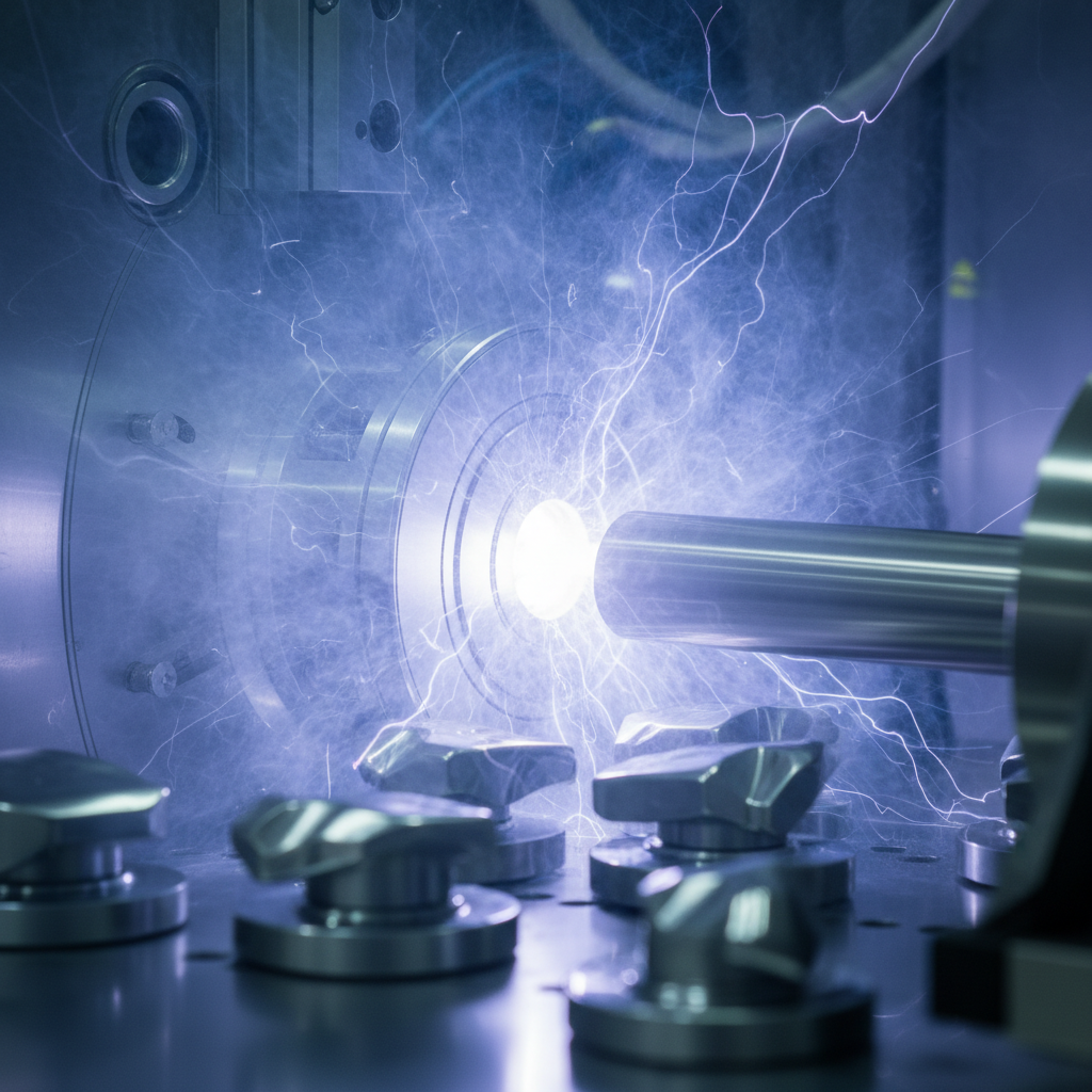
Plasma‑enhanced physical vapor deposition (PE‑PVD) is a vacuum coating method that uses energized plasma to densify films and improve adhesion at lower temperatures. From our Woodbridge facility at 110 Sharer Rd, Sputtek applies PE‑PVD to extend tool life, reduce friction, and stabilize quality for regulated manufacturers.
By Ron — Sputtek • Last updated: June 7, 2026
At a Glance: What You’ll Learn
This guide defines plasma‑enhanced PVD, explains how it works, compares leading methods, and shows when to choose it over conventional PVD or PECVD. You’ll get practical parameters, QA checkpoints, case examples, and best practices drawn from Sputtek’s in‑house coating and QC workflows.
- Plain‑English definition of plasma‑enhanced physical vapor deposition (PE‑PVD)
- When PE‑PVD beats conventional PVD and where PECVD still fits
- Actionable process ranges: pressure, bias, temperature, and rate
- Method breakdowns: ion plating, bias‑assisted sputtering, HIPIMS, and hybrids
- Real‑world examples from automotive, die casting, machining, and pharma tooling
- Quality gates you can copy for stable, repeatable coating performance
Want background on core methods? See our concise PVD types overview and our DLC coating guide for friction control on tools and components.
What Is Plasma‑Enhanced Physical Vapor Deposition (PE‑PVD)?
Plasma‑enhanced PVD is a family of PVD processes that add ionization and substrate bias to energize arriving atoms. The result is denser films, stronger adhesion, and useful properties at lower substrate temperatures than conventional PVD—ideal for heat‑sensitive alloys, tooling, and finished components.
In standard PVD, material is evaporated or sputtered and condenses on a part. In plasma‑enhanced modes, a glow discharge ionizes vapor and a negative bias accelerates ions into the surface, compacting the film and promoting intermixing at the interface.
- Typical vacuum: 0.1–5 Pa during deposition for sputter processes; up to 10−2 Pa base pressure pre‑process.
- Substrate bias: −50 to −300 V for general tooling; higher for intense densification with HIPIMS pulses.
- Temperature window: ~150–450 °C, enabling sensitive steels, precipitation‑hardened alloys, and tempered molds.
- Deposition rate: 0.1–5 µm/hr depending on target, geometry, and power density.
- Typical film types: TiN, TiAlN, CrN, AlCrN, DLC stacks, and application‑specific multilayers.
For a structured refresher on the foundational techniques, our internal PVD types overview outlines evaporation vs sputtering and how plasma assistance changes growth mechanisms.
Why Plasma‑Enhanced PVD Matters for Manufacturers
PE‑PVD improves adhesion, density, and microstructure at lower heat input, translating to longer tool life, more stable Cp/Cpk, and fewer unplanned stoppages. It solves common pain points—wear, galling, and inconsistent finishes—without redesigning parts or over‑tempering heat‑treated substrates.
- Extend tool life: Dense TiAlN or AlCrN typically delivers 1.5–3× life on high‑speed steel drills and carbide inserts under dry or MQL conditions.
- Fight galling and buildup: CrN and DLC topcoats reduce sticking on stainless, aluminum, and coated steels, aiding clean release in stamping and forming.
- Preserve base properties: Lower process temperatures help retain hardness and dimensional stability in tempered dies and molds.
- Stabilize quality: Tighter thickness uniformity (±5–10%) and improved adhesion reduce scrap and rework.
- Regulatory alignment: Repeatable, documented processes support ISO 9001:2015 systems and nuclear vendor expectations for traceability.
These outcomes map directly to Sputtek’s mission: engineered surface performance that extends life, improves wear resistance, and maximizes throughput for automotive, aerospace, oil & gas, nuclear, medical, pharma, and food & packaging operations.
How Plasma‑Enhanced PVD Works (Process Flow)
PE‑PVD adds ionization and substrate bias to a conventional PVD cycle. After precision cleaning, parts enter high vacuum, undergo plasma activation/etch, then receive a dense, adherent film grown by ion‑assisted evaporation or sputtering under controlled pressure, bias, and temperature.
| Step | Purpose | Typical Controls |
|---|---|---|
| 1) Pre‑clean & prep | Remove oils/oxides; set surface energy/roughness | Multi‑stage degrease, microblast; Ra per spec (e.g., 0.05–0.2 µm) |
| 2) Load & pumpdown | Outgas; reach clean base vacuum | Base ≤ 1×10⁻³ Pa; dry pump + turbo |
| 3) Plasma activation/etch | Desorb/activate surfaces; promote adhesion | Ar/H2 plasma; −100 to −800 V bias; 1–5 min |
| 4) Nucleation layer | Seed a compliant, adherent interface | Ti/TiN or Cr; low power first 30–120 s |
| 5) Bulk growth (PE‑PVD) | Build dense, functional thickness | 0.1–5 Pa; −50 to −300 V; 150–450 °C |
| 6) Topcoat/functional layer | Tune friction/thermal/chemical response | AlCrN, CrN, DLC top; 0.5–4 µm total |
| 7) Cool, vent, QA | Prevent moisture shock; verify spec | Thickness mapping, adhesion, hardness, friction |
To differentiate terms: PE‑PVD uses plasma to energize physical deposition. PECVD relies on chemical precursors cracked by plasma, often at even lower temperatures but with different film chemistries and hydrogen content. Both leverage plasma; only PE‑PVD preserves PVD’s physical transport mechanism.
Types of Plasma‑Assisted PVD Methods (and When to Use Them)
Common plasma‑assisted PVD methods include ion plating, bias‑assisted magnetron sputtering, HIPIMS, and hybrid PVD/PECVD stacks. Selection depends on substrate heat limits, adhesion risk, geometry, and target properties like hardness, oxidation resistance, or low friction.
Ion plating (evaporation with energetic assistance)
- How it works: Evaporated species are ionized; substrate bias accelerates them into the surface, compacting the film.
- Best for: Complex, high‑aspect geometries on molds, orthopedic tools, or forming dies where line‑of‑sight limits sputter coverage.
- Notes: High adatom mobility promotes dense TiN/TiCN; moderate temperature (~250–450 °C) maintains temper of many tool steels.
Bias‑assisted magnetron sputtering
- How it works: Plasma ions eject atoms from a target; a controlled negative bias densifies growth and improves step coverage.
- Best for: Cutting tools and dies requiring tough AlCrN/TiAlN with good edge retention and oxidation resistance.
- Notes: Lower substrate temperatures (~200–400 °C) than pure evaporation, with excellent adhesion after Ar/H2 ion etch.
HIPIMS (high‑power impulse magnetron sputtering)
- How it works: Short, high‑current pulses create a highly ionized sputter flux; pulsed bias drives exceptional densification.
- Best for: Demanding adhesion on difficult alloys, sharp edges, and dense AlCrN or CrN underlayers for DLC stacks.
- Notes: Often lower rate than DC sputter but higher density/adhesion; useful for thin, hard interlayers before DLC.
Hybrid PVD/PECVD stacks
- How it works: Combine PE‑PVD hard underlayers with PECVD top seals or DLC for friction control.
- Best for: Release behavior in aluminum die casting/extrusion and low‑friction medical or pharma tooling.
- Notes: Hybrids balance heat input, density, and chemistry. DLC stacks can reach friction coefficients ~0.1 in dry contact.
Looking for a plain‑language background on method families? Our PVD types overview breaks down evaporation vs sputter options before you layer in plasma assistance.
Best Practices for Tools, Dies, Molds, and Components
In Woodbridge, within the Regional Municipality of York, the most reliable PE‑PVD runs follow strict preparation, fixture design, plasma activation, and post‑coat QA. The payoff is predictable life extension, cleaner release, and tighter dimensional control across large batches and prototypes alike.
Preparation and fixturing that prevent failures
- Control surface finish: Target Ra 0.05–0.2 µm for cutting edges; slightly higher for forming dies to anchor films.
- Round critical edges: Micro‑hone cutting edges (e.g., 10–20 µm) to reduce stress risers under hard films.
- Use conductive, line‑of‑sight fixturing: Ensure bias continuity; minimize shadowing with rotation and planetary motion.
- Clean aggressively: Multi‑stage degrease, ultrasonic, microblast, and hot vacuum bake to suppress outgassing.
Process controls that correlate with life
- Bias discipline: Keep within the validated window for each alloy and geometry; excessive bias can embrittle sharp edges.
- Temperature limits: Stay under temper draw temperatures; log part thermocouples on first‑article runs.
- Thickness targeting: Typical 1–3 µm for cutting tools; 2–4 µm for forming/stamping, tuned to radius and load.
- Rotate intelligently: Program dwell/rotation to equalize coverage on deep features and cavities.
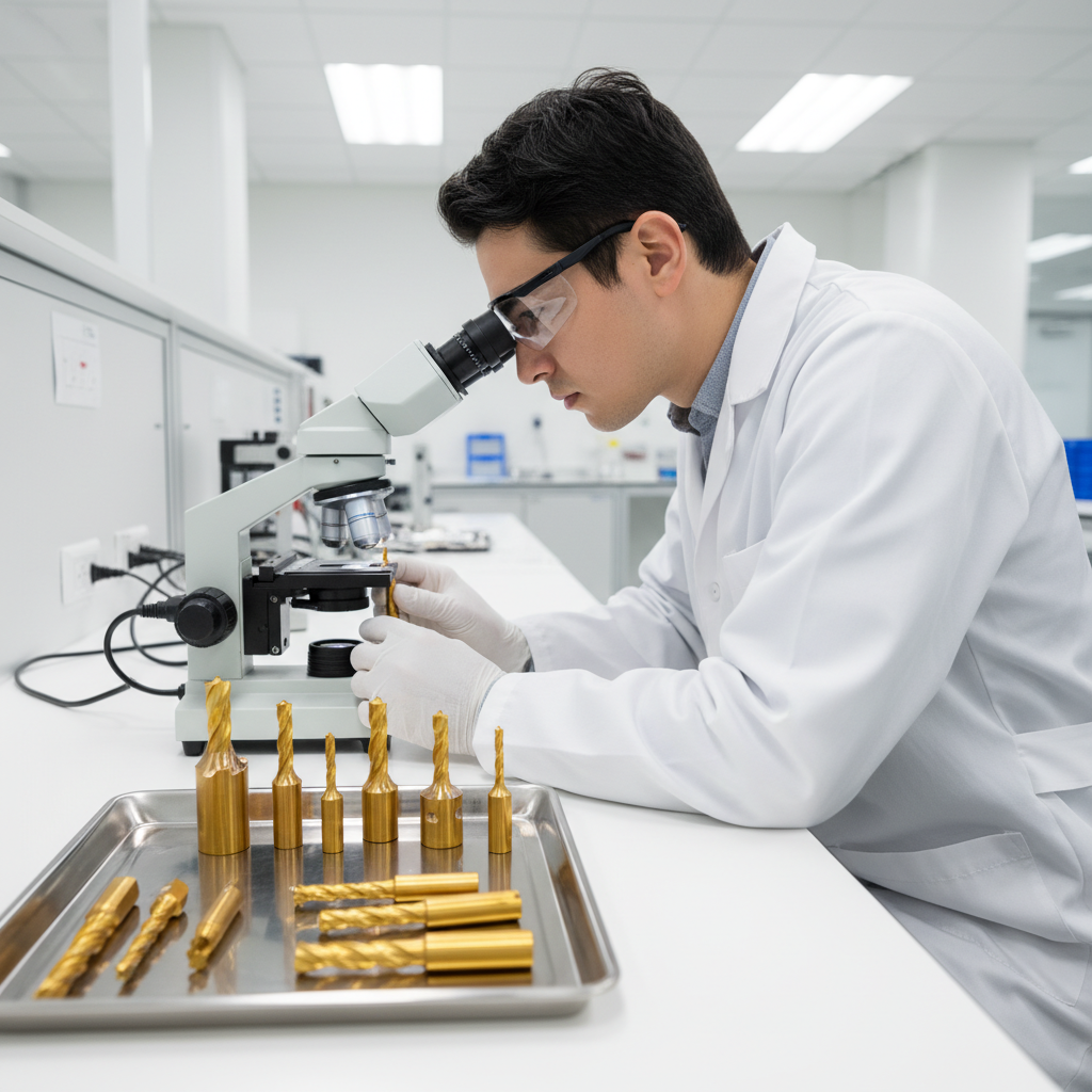
Quality checks that catch issues early
- Adhesion: Scratch or Rockwell indentation mapping by zone; look for consistent crack patterns.
- Thickness: XRF or calo to confirm ±5–10% uniformity across critical faces.
- Hardness and friction: Nanoindentation for modulus/hardness; tribo for friction if low‑µ is critical.
- Documentation: Batch travelers, fixture recipes, and post‑process photos support ISO 9001/traceability.
Local considerations for Woodbridge
- Plan pickups near SmartCentres Woodbridge to align with shift changes and minimize truck idle time.
- Build schedule slack in winter; cold starts and humidity swings can extend vacuum pumpdown and thermal stabilization.
- Coordinate with Weston Rd / Highway 7 transit windows to avoid rush‑hour congestion for just‑in‑time tooling.
For friction‑critical applications, our DLC coating guide explains when a DLC top stack on PE‑PVD underlayers is advantageous for release, galling resistance, and tribology.
Tools, Systems, and Resources You Can Use
Deploy proven hardware and QA methods: high‑capacity multi‑cathode PVD chambers, programmable bias supplies, calibrated thickness tools, and an in‑house QC lab. Pair them with validated recipes for TiN, TiAlN, AlCrN, CrN, and DLC stacks on your primary alloys.
Sputtek operates multiple production PVD systems and a Thermospray cell in a modern, 15,000 sq ft facility. Our SPUN 2,000 and SPUN 4,000 class systems handle up to four‑digit‑part counts per batch, with rotation/planetary motion for uniformity on complex geometries. We complement this with sandblasting, microblasting, degreasing, stripping/polishing, lapping, and a QC laboratory.
- Recipe building blocks: Ar/H2 etch, Ti or Cr adhesion layers, and application‑driven topcoats (TiAlN, AlCrN, CrN, DLC).
- Measurement kit: XRF thickness (µm), nanoindentation (GPa), scratch/indent adhesion, optical profilometry (Ra/Rz).
- Release and low‑µ: DLC overlays can reach friction ~0.1 in dry contact, with underlayers tuned for load and heat.
- Training and SOPs: Operator work‑instructions tied to product families reduce drift and help maintain Cp/Cpk over time.
Note: Plasma deposition is not the same as plasma cutting. If you’re searching for cutting equipment, that’s separate fabrication hardware (see examples of plasma cutting hardware). Here we focus on vacuum deposition for engineered thin films.
Case Studies and Practical Examples
PE‑PVD consistently improves life and stability across tools and components. The following mini‑scenarios reflect patterns we see when partnering with manufacturers from prototype to high‑volume production.
Automotive stamping: stainless draw die release
- Problem: Galling on 300‑series stainless led to 2–3 unplanned stoppages per week and visible scuffing.
- Approach: CrN underlayer by bias‑assisted sputter plus thin DLC top to lower friction; targeted 2.5–3.0 µm total.
- Result: Cleaner release, smoother finish, and a shift from weekly to monthly maintenance windows.
Aluminum die cast: soldering and stuck pins
- Problem: Aluminum pickup on core pins and dies forced frequent solvent cleaning and part rejection.
- Approach: AlCrN by HIPIMS underlayer for dense adhesion; optional carbon‑rich seal; validated at 200–350 °C.
- Result: Noticeably less buildup and improved shot‑to‑shot consistency during extended runs.
Machining: carbide drills on hardened steels
- Problem: Edge chipping and premature failure when dry drilling 50–60 HRC steels.
- Approach: TiAlN via bias‑assisted sputter at 2 µm; edge hone ~15 µm; validated rotation to equalize shank/flute coverage.
- Result: Typical 1.5–2.5× life extension and cleaner hole quality under dry or MQL conditions.
Pharma tooling: low‑adhesion tablet punches
- Problem: Stick‑slip and cosmetic pickup on lettering features.
- Approach: Polished CrN with thin DLC overlay; tight control of thickness on relief features.
- Result: Smoother ejection and reduced cleaning between batches.
If you’re exploring DLC specifically, our DLC coating guide breaks down stack architectures and when to choose DLC versus hard nitrides.
Plasma‑Enhanced PVD: Frequently Asked Questions
These concise answers address the most common questions we hear from manufacturing engineers, toolmakers, and quality leaders evaluating plasma‑assisted PVD for production.
What’s the difference between PE‑PVD and PECVD?
Both use plasma, but PE‑PVD transports material physically from a solid target, while PECVD forms films from chemical precursors cracked in plasma. PE‑PVD tends to yield denser nitrides/carbides with strong adhesion; PECVD enables very low‑temperature deposition and different chemistries, including some DLC variants.
How thick should plasma‑enhanced PVD coatings be?
Most tooling runs well at 1–3 µm for cutting edges and 2–4 µm for forming and stamping surfaces. Tight corners and small radii benefit from thinner, denser layers to avoid stress concentration. Validate thickness by XRF or calo and map uniformity on critical faces.
Will PE‑PVD affect my heat‑treated hardness?
It’s designed to protect it. Plasma‑assisted PVD typically runs ~150–450 °C, below temper draw for many tool steels. We log part temperatures on first articles and set guard limits to preserve base hardness and dimensional stability.
What industries benefit most from plasma‑enhanced PVD?
Automotive stamping and die cast, aerospace machining, oil & gas wear parts, nuclear components, medical devices, pharma tooling, and food & packaging equipment all see gains in wear, release, and process stability when PE‑PVD is specified and controlled.
Is plasma the same as plasma cutting?
No. Plasma cutting is a fabrication process that uses a high‑temperature plasma arc to cut metal. PE‑PVD is a vacuum coating process using low‑pressure plasma to grow thin films. If you need cutting hardware, see examples of plasma cutting hardware.
Key Takeaways and Next Steps
PE‑PVD delivers dense, adherent, application‑tuned films at lower heat input. Pair disciplined prep, bias control, and QA with the right nitride, carbide, or DLC stack to stabilize quality and extend life across tools, dies, molds, and components.
- Plasma‑enhanced physical vapor deposition densifies films, enabling strong adhesion at moderate temperatures.
- Choose among ion plating, bias‑assisted sputter, HIPIMS, and hybrid stacks based on alloy, heat limits, and target properties.
- Validate with thickness, adhesion, and hardness mapping tied to fixtures and recipes.
- Use DLC overlays where friction and release dominate performance needs.
Ready to evaluate parts? Share drawings, alloy, current issues, and success criteria. We’ll propose a plasma‑assisted PVD stack and validation plan. For foundational context, review our PVD types overview and DLC coating guide.
Reliable coatings ride on rigorous measurement. For an example of analytical discipline in materials labs, see this overview of lab analysis evolution and a primer on molecular weight and PDI concepts—different domains, same measurement mindset we apply in our QC workflows.
Plasma also appears in biomedical contexts, but those are unrelated to vacuum coatings. If you encounter “plasma” in life‑sciences, it refers to an entirely different medium (see a general proteomics example), not the low‑pressure glow used for thin films.


