Physical vapor deposition companies are specialized coating providers that deposit ultra-thin, high-hardness films in vacuum to cut friction and wear on tools and components. In Woodbridge, teams use PVD to extend service life, steady quality, and reduce changeovers. The right partner delivers adhesion, thickness control, and repeatability at scale for production results you can trust.
By Ron — Sputtek
Last updated: 2026-06-24
At a Glance: What You’ll Learn
Use this complete guide to evaluate physical vapor deposition companies with confidence. You’ll learn what PVD is, how it works, key methods, how to compare vendors, and best practices. Apply the checklists to align engineering targets, qualify suppliers, and boost tool life and throughput.
This guide is written for manufacturing engineers, tool and die shops, quality leaders, and procurement teams. You’ll find actionable criteria and examples drawn from automotive, medical, nuclear-adjacent, and food and packaging programs supported by Sputtek’s engineering team in the Greater Toronto Area.
- Clear definition of PVD and how it differs from other deposition methods
- How PVD films like TiN, CrN, AlTiN, and DLC behave in production
- Step-by-step overview of the process from prep to post-finishing
- Vendor comparison criteria, red flags, and a reusable scorecard
- Application-specific guidance for dies, molds, cutters, and components
- Local logistics tips for Woodbridge teams coordinating coating runs
What Is Physical Vapor Deposition (PVD)?
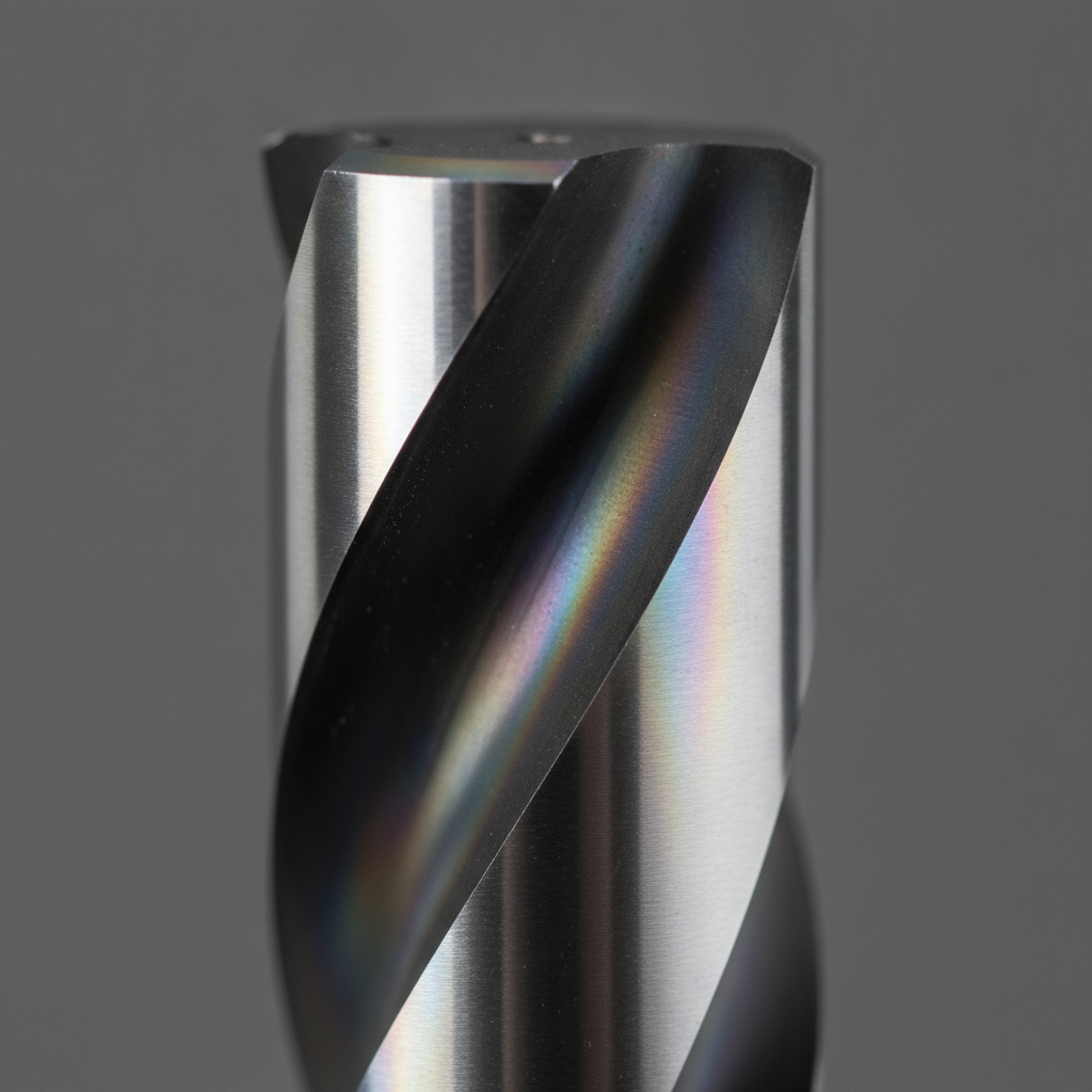
Physical vapor deposition is a vacuum coating process that transforms solid materials into vapor and condenses them as dense, bonded films 0.5–5 μm thick. These engineered layers deliver high hardness, strong adhesion, and low friction—extending tool life and stabilizing tolerances under demanding duty cycles.
PVD covers methods such as sputtering and cathodic arc. Typical films include TiN, TiCN, AlTiN, CrN, and DLC. Hardness commonly exceeds 2,000 HV; coefficients of friction can drop below 0.2 with DLC on proper substrates. Because thickness is microns—not millimeters—critical fits and edges remain in tolerance.
- High hardness with resilience: Multilayer nano-structures resist abrasion and micro-chipping in 0.5–3 μm ranges.
- Thermal behavior: AlTiN stacks retain performance above 800°F on high-speed cutting; CrN supports corrosion resistance on molds.
- Surface energy control: DLC improves release and reduces built-up edge on nonferrous cuts and forming.
- Clean process: Vacuum deposition avoids wet chemistries and minimizes contamination risk.
PVD vs. CVD vs. Thermal Spray
Choosing the correct process is about thickness, temperature, and duty cycle.
- PVD: 0.5–5 μm, lower thermal load, excellent for precision tools/components.
- CVD: 5–15 μm, higher temperatures, strong diffusion layers for heavy cutting.
- Thermal spray/HVOF: 50–500+ μm, bulk build for impact, repair, and barrier layers.
For deeper background on finish selection and stacks, see our internal primer on PVD types and finishes, which explores nitrides, carbides, and hybrid architectures.
Why the Right PVD Company Matters
Coatings don’t succeed by recipe alone. The provider’s prep discipline, fixturing, chamber control, and QC make adhesion and thickness repeatable. That reliability reduces scrap, improves run length, and protects tight tolerances across batches.
We’ve found that early failures usually trace to surface prep, masking gaps, or poor line-of-sight. End-to-end vendors that control blasting, cleaning, masking, deposition, and post-coat lapping remove variables and keep edge build consistent. Batch-to-batch variation tightens when fixtures and rotation are engineered for each geometry.
- Adhesion: Cross-hatch, Rockwell, or scratch tests confirm bond integrity on your alloys.
- Thickness control: 1.0–2.5 μm windows are common; mapping verifies uniformity on critical faces.
- Roughness targets: Many sealing surfaces require Ra ≤ 0.1–0.2 μm; plan pre-polish and post-lapping.
- Documentation: PPAP, lot traceability, and recipe change control prevent surprises during launches.
Risks When Vendor Fit Is Poor
- Edge flaking: Often from inadequate rounding or over-thick builds on sharp features.
- Color shift: Indicates recipe or gas ratio drift; correlates with property changes.
- Inconsistent release: Tied to roughness or inappropriate topcoat selection on molds.
What Buyers Usually Miss
- Fixture design: It governs line-of-sight and micro-shadowing; rotation speeds matter.
- Cleaning validation: Residual oils or blasting media cause pinholes and adhesion loss.
- Thermal budget: Some tool steels temper back above 400°F; recipes must respect this.
As Canada’s largest PVD/DLC service provider, Sputtek operates multiple systems and a Thermospray cell in a 15,000 sq ft Woodbridge-area facility, supporting prototypes to high-volume batches with ISO 9001:2015 and Nuclear N299.3 approvals. That capacity steadies queues and supports campaign planning.
How PVD Works: A Practical Walkthrough
PVD loads cleaned, fixtured parts into a vacuum, energizes a solid target to create a vapor, and condenses that vapor on the parts as a dense film. Substrate biasing, temperature, rotation, and gas ratios tune hardness, friction, color, and growth rate.
Here is the typical production sequence:
- Pre-clean and roughness prep: Degrease, ultrasonic clean, and sandblast/microblast to the target Ra. Verify with QC.
- Mask and fixture: Protect sealing faces; design fixtures for line-of-sight; validate rotation and spacing.
- Vacuum and heat: Pump down to high vacuum; heat to stabilize the substrate (often 200–500°F depending on alloy).
- Ion clean: Sputter-etch to activate the surface; form adhesion interlayers as needed.
- Deposit: Sputter or arc-evaporate targets; introduce reactive gases to form nitrides/carbides/oxides.
- Grow to spec: Control bias and gas ratios; build 0.5–5 μm depending on tolerance budget.
- Cool and verify: Thickness measurement (calo, XRF), adhesion check, color/appearance inspection.
- Post-finish: Lapping/polishing to dial Ra/Rz for release and sealing.
Controls That Drive Results
- Substrate bias (V): Densifies films; too high can embrittle thin edges.
- Gas flow (sccm): Tunes stoichiometry; affects color and hardness.
- Rotation (rpm): Evens thickness on complex features and vents.
- Cooling rate (°F/min): Manages stress and color consistency on stacks.
Common Defects and Prevention
- Pinhole density: Improve cleaning validation and pre-sputter etch time.
- Edge overbuild: Adjust fixture spacing and angle; consider pre-radius or lapping.
- Arc droplet artifacts: Use filtered arc or hybrid sputter-over-arc stacks.
For a deeper dive on process flow and finish trade-offs, our PVD process overview maps each step to the measurements that matter on the factory floor.
Types, Methods, and Approaches
Sputtering, cathodic arc, and hybrid stacks cover most needs. TiN/TiCN/AlTiN support high-temperature cutting; CrN balances corrosion resistance and polishability; DLC drives very low friction for sliding and release. Selection depends on substrate, geometry, and duty cycle.
Sputtering
- Precise thickness control with excellent uniformity on complex shapes.
- Wide chemistry: nitrides, carbides, oxides, DLC variants.
- Great for molds, medical instruments, and dimensionally tight components.
Cathodic Arc
- High deposition rate and very dense films for aggressive wear.
- Modern filtered systems reduce macroparticles; hybrids add smoothness.
- Ideal for cutting tools, forming dies, and impact-prone edges.
Diamond-Like Carbon (DLC)
- Coefficient of friction often < 0.2 on nonferrous cuts and sliders.
- Excellent anti-stick behavior in stamping and plastic processing.
- Frequently layered over adhesion/barrier stacks for durability.
Color, Finish, and Measurement
- Color cues: TiN (gold), CrN (silver-gray), AlTiN (charcoal-violet), DLC (black).
- Finish: Many sealing surfaces target Ra ≤ 0.1–0.2 μm after lapping.
- Thickness: 1–3 μm is common for tools; components vary by fit and load.
When you need thicker build, impact resistance, or dimensional restoration, pair PVD with thermal spray or HVOF. Sputtek supports Thermospray (including Pulsed HVOF) alongside PVD to tailor coverage across tool families, minimizing changeovers and rework.
How to Compare Physical Vapor Deposition Companies
Evaluate PVD partners by certifications, in-house prep and post-processing, coating portfolio, capacity, fixturing expertise, and QA documentation. Prioritize adhesion data on your alloys and pilot results over generic datasheets.
| Selection factor | What “good” looks like | Why it matters |
|---|---|---|
| Quality system | ISO 9001:2015; sector approvals (e.g., N299.3) | Auditable processes and traceability reduce risk |
| In-house capabilities | Blasting, cleaning, masking, stripping, lapping, QC | Fewer hand-offs, steadier adhesion and finish |
| Application coverage | Tools, dies, molds, components, complex alloys | Faster engineering cycles and fewer no-quotes |
| Capacity | Multiple chambers; large-batch fixtures | Shorter queues and campaign scheduling |
| Documentation | PPAP, thickness maps, adhesion tests | Smoother launches and supplier audits |
- Ask for adhesion tests: Scratch or cross-hatch data on your heat-treated alloys.
- Run a representative pilot: Mix edge radii and cavity depths to stress the recipe.
- Inspect fixturing: Confirm line-of-sight, rotation, and vent handling.
For finishing nuances and appearance control, our PVD finishing guide explains how lapping, polish, and stack design interact to hit surface energy targets without compromising tolerance.
Best Practices for Engineering, QA, and Procurement
Define performance targets, share substrate and finish data, and lock acceptance criteria before scaling. Pilot on representative parts. Then control recipe changes, fixtures, and prep steps with documented QC to protect results across batches.
Engineering Handoff
- List alloy, heat treat, and temper sensitivity; set allowable substrate temperature.
- Call out masking areas, sealing faces, and critical dimensions with tolerance budgets.
- Provide duty cycle: load, speed, mating materials, and operating temperature ranges.
- Specify target roughness (e.g., pre-coat Ra 0.05–0.1 μm; post-coat Ra ≤ 0.2 μm).
QA Checkpoints
- Thickness method (XRF/calo), mapping plan, and acceptance window (e.g., 1.5 ±0.5 μm).
- Adhesion method and limits (scratch, Rockwell indents, or cross-hatch).
- Surface finish before/after; micrographs on first articles for stack validation.
- Lot traceability and non-conformance handling with containment steps.
Procurement Controls
- Document change control: recipe edits, target sources, fixture revisions.
- Schedule windows aligned to production campaigns; define expedite criteria.
- Use a scored supplier questionnaire and a shared action log for improvements.
Local considerations for Woodbridge
- Coordinate drop-offs near SmartCentres Woodbridge to bundle errands with other vendors in the area.
- Model-year rollover ramps demand; book coating windows before summer peaks to avoid bottlenecks.
- Aim deliveries around Weston Rd / Highway 7 off-peak times to keep tooling moving efficiently.
For stack selection ideas and common trade-offs across alloys and geometries, our PVD plating overview outlines when to prefer nitrides, carbides, or DLC and how to plan for post-coat finishing.
Tools, Standards, and Resources
Use recognized quality standards, supplier questionnaires, and a simple scorecard to compare PVD companies. Certification evidence, test records, and application notes are stronger than color charts or generic property tables.
Scorecard You Can Reuse
- Quality (25%): ISO 9001:2015; sector approvals; audit history.
- Process (25%): In-house prep, fixtures, change control, and QC lab capability.
- Application fit (25%): Proven stacks for your alloys and duty cycles.
- Capacity (15%): Multiple systems, large-batch options, turnaround discipline.
- Support (10%): Engineering responsiveness, pilot guidance, documentation.
Evidence That Matters
- Thickness maps and adhesion tests from prior runs on similar alloys (1–3 μm target, method noted).
- First-article micrographs and roughness before/after lapping (Ra 0.05–0.2 μm typical).
- Recipe and fixture traveler with revision control.
Case Studies and Practical Examples
When coatings are engineered with clean prep, solid fixtures, and the right stack, results follow quickly: smoother cycles, longer runs, and steadier dimensions. These examples reflect common duty cycles our Woodbridge team supports from prototype to volume.

Automotive stamping dies (AHSS and coated sheet)
- Pain point: Galling on radii and binder surfaces cutting uptime by mid-run.
- Approach: CrN base with DLC on slides; pre-radius edges; post-lap to Ra ≤ 0.2 μm.
- Result: Smoother draw, fewer pulls, more stable campaigns across 1–3 μm builds.
Plastic injection molds (gates, cores, vents)
- Pain point: Sticking in gated features and vent fouling affecting finish.
- Approach: CrN with controlled roughness; DLC on slides and pins; mapped thickness.
- Result: Improved release and cycle consistency; less reliance on chemical sprays.
Cutting tools (aluminum and abrasive alloys)
- Pain point: Built-up edge on nonferrous; rapid wear on abrasive materials.
- Approach: DLC for nonferrous cuts; AlTiN/TiCN layers for heat and abrasion.
- Result: Better edge retention and thermal management; steadier dimensional control.
Precision components (sliding pairs and valves)
- Pain point: Stick-slip and fretting on mating surfaces.
- Approach: DLC with pre-polish to Ra 0.05–0.1 μm; tight 1–2 μm targets.
- Result: Lower friction and wear; improved service intervals in operation.
Need a second set of eyes on a coating challenge? Book a quick engineering consult to review substrates, tolerances, and duty cycles. We’ll suggest a pilot and acceptance criteria you can validate on real parts.
Frequently Asked Questions
These short answers cover the questions we hear from engineering, QA, and sourcing teams when vetting PVD companies. Use them to reduce delays and align expectations before you pilot.
What’s the fastest way to qualify a new PVD supplier?
Pilot on a representative mix of parts. Define acceptance for adhesion, thickness, and finish. Inspect fixtures and rotation. Lock the recipe and traveler once results meet targets, then scale to production.
How do I choose between DLC, CrN, and AlTiN?
Match the coating to duty cycle and substrate. Use DLC for low friction and release on nonferrous or sliding pairs, CrN for corrosion resistance and polishability, and AlTiN/TiCN for high-temperature cutting and abrasion.
Can PVD handle tight-tolerance, complex features?
Yes—with the right fixtures and process. Sputtering delivers strong uniformity. Document pre-coat finish, target 1–3 μm builds, and plan post-coat lapping for sealing or optical faces.
When is thermal spray or HVOF a better fit than PVD?
Choose thermal spray or HVOF when you need thick build, impact resistance, or dimensional restoration. PVD excels at thin, hard, low-friction films for precision tools and components. Many factories deploy both across different parts.
Conclusion and Next Steps
Selecting a PVD partner is an engineering decision. Define targets, validate with pilots, and favor certified, end-to-end providers. The payoff is longer tool life, steadier throughput, and fewer surprises in production.
- Key takeaways: Align targets, pilot first, lock the recipe, then scale with change control.
- Action steps this week: Build a one-page spec, request adhesion data, and schedule a pilot.
- Where to learn next: Our PVD process overview and finishing guide unpack the measurements that matter.
Related Articles and Deep Dives
Deepen your understanding of deposition, stacks, and finish control to choose the right approach per part family. The following internal resources expand on process flow, finish choices, and application trade-offs.
To explore how film architecture drives performance, see our discussion on types of PVD. For appearance and surface energy control, revisit the PVD finishing guide. If you’re deciding between nitrides, carbides, and DLC for complex tools, our PVD plating overview breaks down practical choices by duty cycle.


