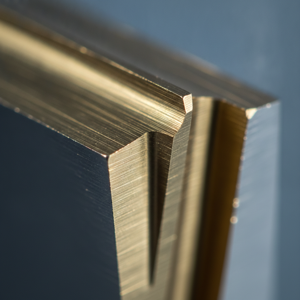
PVD coating is a vacuum thin-film process that deposits hard, wear-resistant layers such as TiN, TiAlN, CrN, and DLC onto tools and components. Typical thickness is 1–5 μm with hardness up to 3,500 HV and low friction. For Woodbridge manufacturers, it’s a proven way to extend tool life, stabilize quality, and reduce downtime.
By Ron — Sputtek | Last updated: 2026-06-29
At a Glance: Summary
PVD coating improves wear resistance, reduces friction, and increases part life using hard, thin films deposited in a vacuum. Expect 1–5 μm thickness, low friction (as low as ~0.1 for DLC), and excellent adhesion. For production teams, that means longer maintenance intervals, fewer scrap parts, and more predictable throughput.
This guide is built for manufacturing engineers, toolmakers, and operations leaders who need fast, practical answers about physical vapor deposition. You’ll learn what PVD is, when to use it, how it’s done, which chemistries to choose, and how Sputtek supports prototype-to-volume programs from its ISO 9001:2015-approved Woodbridge operation.
- What PVD is and how it works in plain terms
- Where PVD beats alternatives like CVD or HVOF
- Common chemistries (TiN, TiCN, TiAlN, CrN, DLC) and use cases
- Design, prep, fixturing, and QA best practices
- Step-by-step process, cycle times, and temperature windows
- Real examples from stamping, machining, molds, and die casting
Contents
- What is PVD coating?
- Why PVD coating matters in Woodbridge
- How the PVD process works
- Types of PVD coatings and selection
- Best practices and QA
- Tools and resources
- Case studies and examples
- FAQ
- Conclusion and next steps
What Is PVD Coating?
Physical Vapor Deposition (PVD) is a vacuum process that transforms solid coating materials into a vapor and condenses them onto parts as ultra-thin, dense films. The result is 1–5 μm coatings with high hardness, strong adhesion, and tailored tribology for demanding production environments.
In practice, PVD uses a sealed vacuum chamber where coating targets (e.g., titanium, chromium, carbon sources) are energized to release atoms or ions. These react with gases like nitrogen, acetylene, or argon and condense on parts arranged on rotating fixtures. Deposition temperatures typically range 150–500 °C depending on chemistry and substrate.
- Typical hardness ranges: TiN ~2,000–2,200 HV; TiAlN up to ~3,200 HV; DLC effective friction ~0.1–0.2.
- Coating thickness: often 1–5 μm (decorative layers may be thinner; heavy-duty tools sometimes 5–8 μm).
- Cycle duration: commonly 4–12 hours, varying by batch size, substrate mass, and desired thickness.
Coating is one of the most overloaded words in industry. Many consumer references point to automotive ceramic sealants or floor epoxies, which are entirely different from PVD thin films used in manufacturing. For example, consumer ceramic car coatings or even general residential floor coatings are not comparable to vacuum-deposited, micron-scale engineering films. Some consumer FAQs discuss coatings over PPF films (e.g., ceramic over PPF)—again, a different domain than industrial PVD.
Why PVD Coating Matters to Woodbridge Manufacturers
PVD coating reduces tool wear, friction, and built-up edge, directly improving uptime and part consistency. In high-mix or high-volume plants, it stabilizes cycle time, lowers scrap, and makes quality more predictable—critical for meeting OEM schedules and audits.
In our experience supporting automotive, aerospace, medical, and packaging lines, the biggest wins are reliability and repeatability. When a stamping die or end mill lasts 2–5× longer, preventive maintenance becomes predictable. That shift cuts unplanned stoppages and helps teams hit takt time. For several Woodbridge toolrooms, adding TiAlN or DLC on cutting edges eliminated early edge chipping and heat checking.
- Friction and sticking: DLC’s effective friction can approach 0.1 on lubricated pairs, reducing scuffing during dry or boundary-lubed runs.
- Surface integrity: A 1–3 μm film changes near-surface tribology without altering the core strength or geometry of precision tools.
- Temperature resilience: AlTiN/TiAlN withstand hot cutting and stamping; CrN suits corrosion-prone, washdown, or food-contact hardware.
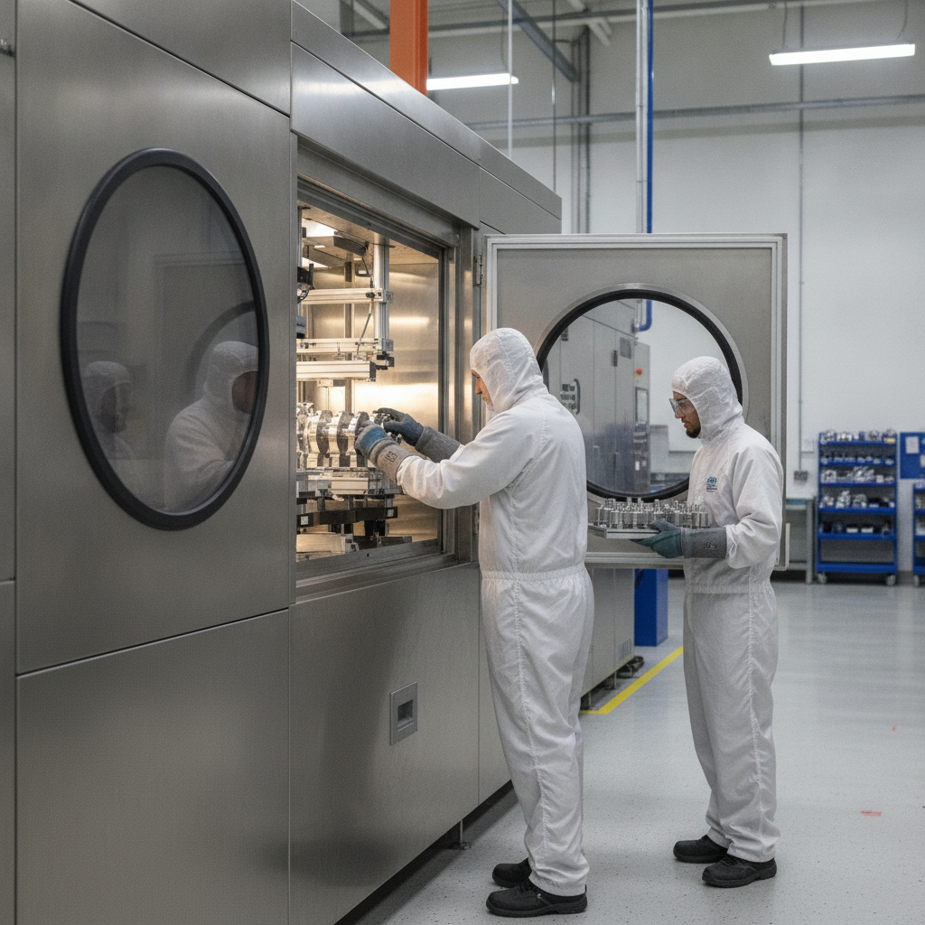
Sputtek’s engineering-led approach includes in-house sandblasting, microblasting, degreasing, stripping, polishing, lapping, and a QC lab. High-capacity SPUN systems support loads up to ~1,200 kg/cycle (SPUN 2,000) and ~3,000 kg/cycle (SPUN 4,000), enabling stable scale-up from pilot to full production without recipe drift.
Local considerations for Woodbridge
- Plan pickups and drop-offs outside peak traffic near Weston Rd / Highway 7 to minimize logistics time for heavy tooling and components.
- Schedule heat-sensitive substrates during cooler months when ambient handling is easier; reserve higher-temperature chemistries (e.g., TiAlN) when substrates allow.
- For urgent turnarounds, coordinate batch consolidation; teams near SmartCentres Woodbridge often combine similar alloys to streamline prep and fixturing.
How the PVD Coating Process Works (Step-by-Step)
PVD coating follows a controlled sequence: surface prep, fixturing, pump-down, plasma cleaning, deposition, cool-down, and QC verification. Each step protects adhesion and thickness uniformity, ensuring the 1–5 μm film delivers the expected wear and friction benefits in production.
Even small changes in preparation can alter adhesion. We run all pre-coat steps in-house for control. Below is a practical walkthrough you can map to your own PPAP or validation plan.
- Incoming inspection and cleaning. Verify dimensions, note wear zones. Ultrasonic degreasing removes oils; target Ra roughness baseline as required for bite (e.g., 0.05–0.2 μm after lapping).
- Surface activation. Sandblast or microblast to create anchoring features where appropriate; avoid peening geometries that need edge retention.
- Fixturing and masking. Orient cutting edges and lubricated faces toward the flux; mask bores, datum faces, or fits that must remain bare.
- Pump-down and plasma clean. Pump chamber to high vacuum (commonly 10−3–10−5 mbar). Argon plasma sputter-cleaning removes last monolayers.
- Deposition. Energize targets (e.g., Ti, Al-Ti, Cr, carbon sources). Introduce reactive gases (N2, C2H2) as required. Substrate temperature set to the alloy window.
- Cool-down and unload. Controlled cooling limits thermal shock; parts return near ambient for handling.
- Post-process QA. Microhardness (HV), calotest or XRF for thickness, scratch/adhesion tests (e.g., progressive load 50–100 N), visual inspection under magnification.
Cycle time depends on part mass and load density. Large fixtures and heavy dies add thermal lag and can extend a 6-hour recipe to 9–10 hours. That’s where high-capacity PVD systems matter: stable temperature control across 1,200–3,000 kg loads keeps chemistry consistent from the first to the last part in the batch.
Types of PVD Coatings and When to Use Them
Match chemistry to failure mode. Use TiN for general wear, TiCN for abrasive sliding, TiAlN/AlTiN for hot cutting and stamping, CrN for corrosion and washdown, and DLC for low-friction sliding or molding release. Substrate compatibility and temperature limits guide the shortlist.
Common chemistries
- TiN (gold): ~2,000 HV, great general-purpose wear layer for HSS tools, dies, and fixtures. Often 2–4 μm.
- TiCN (gray/blue): Higher hardness vs. TiN and better abrasion resistance. Useful for sliding wear and some aluminum work.
- TiAlN / AlTiN (violet/dark): Hot-hard layers that resist oxidation; strong pick for high-speed machining and hot stamping.
- CrN (silver): Balanced wear plus corrosion resistance; common on food-grade components and plastic tooling in humid, washdown areas.
- DLC (black): Ultra-low friction (~0.1–0.2), excellent for galling reduction, forming nonferrous metals, and ejection pins in molds.
Process variants
- Sputtering: Great for smooth, dense films and complex alloys; good thickness control.
- Arc evaporation: High ionization and strong adhesion; microdroplets require polish-sensitive applications to be assessed.
- Hybrid systems: Combine arc and sputter targets to balance density, stress, and surface smoothness.
Quick comparison: PVD vs. CVD vs. HVOF
| Method | Typical Thickness | Temp Window | Hardness (indicative) | Best For |
|---|---|---|---|---|
| PVD | 1–5 μm | ~150–500 °C | Up to ~3,500 HV | Precision tools, dies, molds, sliding pairs |
| CVD | 5–20 μm | ~900–1,000 °C | ~2,000–3,000 HV | Carbide inserts needing thick, high-temp films |
| HVOF (thermal spray) | 50–300 μm | Substrate heating modest | Very high density; HV varies by alloy/cermet | Shafts, valves, and repair builds needing thickness |
Sputtek offers both PVD coating and Thermospray (including pulsed HVOF). We frequently combine approaches: for example, HVOF to restore a worn diameter, then a thin PVD topcoat for tribology control. For a deeper dive into carbon-based options, our DLC coating process explainer covers low-friction use cases, and the broader DLC services guide compares variants.
Best Practices: Design, Prep, and Quality Assurance
Great PVD results start before the chamber: specify the failure mode, prepare the surface, fixture for line-of-sight, and validate with hardness, thickness, and adhesion checks. Document the recipe so future batches match the pilot’s performance.
Design and material tips
- Define failure modes: abrasive wear, adhesive galling, heat, or corrosion. Chemistry choice flows from here.
- Mind substrate temp limits: PVD windows (150–500 °C) suit most tool steels and many stainless alloys; consult for aluminum, copper, or hardened maraging steels.
- Edge prep: Small hone (e.g., 5–15 μm) can improve edge life and adhesion on cutting tools.
- Geometry check: PVD adds microns, not millimeters. Confirm fits for components with tight clearances.
- Use a matrix: Keep a simple table correlating failure mode → candidate chemistries → test criteria.
Preparation and fixturing
- Cleanliness: Ultrasonic degreasing plus deionized rinses; final solvent checks. Residual organics are a primary adhesion risk.
- Texture control: For sliding faces, after-coating lapping can reach Ra ~0.02–0.05 μm; polish ejection pins for release.
- Masking and orientation: Keep fits bare; face critical edges toward plasma flux for uniform thickness (±10–15% typical).
- Fixture density: Avoid shadowing by spacing parts; rotate if possible for uniformity on complex geometries.
Verification and documentation
- Thickness checks: XRF, calotest spot checks per part family; typical spec 2–4 μm for tools, 1–2 μm for precision components.
- Hardness/adhesion: Microhardness mapping; scratch tests targeting progressive failure loads (e.g., 60–100 N). Record values with photos.
- Run cards: Keep alloy, surface prep, temperature, gas flow, and time parameters. This makes PPAPs smoother.
We keep these steps in-house—sandblasting, microblasting, stripping, polishing, and a QC laboratory—so the recipe you validate during pilots is the same one used for 3,000 kg production cycles. For broader context across thin films, our metal vapor deposition overview explains how PVD sits within the wider Deposition family.
Tools and Resources You Can Use
Equip your team with a simple toolkit: a failure-mode checklist, a fixturing orientation sketch, and three QC checks (thickness, hardness, adhesion). These small habits ensure each PVD batch performs like the last one.
Shop-floor toolkit
- Failure mode worksheet: Note abrasive zones, heat tint, pickup areas, and corrosion spots with photos.
- Orientation sketch: Mark face/edge orientations and masked areas; include alloy and hardness.
- QC trio: XRF/calotest for thickness, microhardness for film response, and scratch test for adhesion confirmation.
- Recipe card: Capture gas flows, bias, temp, and time so pilots and production match.
Resource library
- DLC reference: Our complete DLC coating guide breaks down low-friction options for forming and molding.
- Process fundamentals: For a wider look at thin films in manufacturing, start with our Deposition cluster primer.
- Application notes: Compare carbon-based choices in the diamond-like coating note if release and anti-galling are key.
Need a working session? We host quick whiteboard reviews that align coatings to your failure Pareto. A 30–45 minute review typically produces a two-run validation plan covering thickness, hardness, and adhesion with clear pass/fail criteria.
Case Studies and Real-World Examples
Across stamping, machining, molding, and die casting, PVD shows repeatable 2–5× tool life gains when chemistry and prep match the failure mode. Below are condensed scenarios we see often in Woodbridge and the GTA.
Automotive stamping die: AHSS galling
A Woodbridge stamper forming AHSS reported heavy pickup on draw beads within 20,000 hits. We applied a hybrid route—microblast + TiAlN on wear zones and DLC on sliding surfaces. Result: galling disappeared for the next 80,000 hits, and planned PM spaced to 100,000+ hits. The maintenance log noted consistent Ra under 0.1 μm after relapping.
End mills on 4140 PH: heat check and edge chipping
Carbide mills lost edges after two production shifts. Switching to AlTiN with a 3 μm spec and a 10 μm edge hone stabilized wear. Tool life jumped roughly 3×; cycle time stayed constant because feed/speed settings held. Scrap from burrs dropped by half on the next three runs.
Plastic injection molds: ejection and release
Ejection pins seized in high-cavitation molds during summer heat. DLC at ~2 μm with post-lap to Ra 0.03 μm solved the stick-slip. Parts released cleanly with no witness marks. Over the quarter, the molder logged unplanned stoppages down by double digits and fewer tip replacements.
Aluminum die cast cores: soldering and washdown
Die cast cores suffered soldering and erosion. CrN at ~4 μm reduced solder adhesion, while periodic washdowns didn’t diminish the layer. The foundry saw more stable surface finish on castings and longer core life between refurb cycles.
Aerospace fastener tooling: adhesive wear
Thread rolling dies exhibited pickup on titanium alloys. TiCN at ~3 μm improved abrasion resistance; a polished exit radius reduced shear. Rolling passes increased per die set, while dimensional drift stayed in spec across validation runs.
Food and packaging knives: washdown corrosion
Stainless knives dulled quickly under frequent washdown. CrN with a post-lap finish maintained edge life and resisted spotting. The plant reported steadier cut quality and fewer changeovers per shift.
Oil and gas valve stems: sliding galling
Stems showed scoring after extended service. A DLC topcoat over a polished substrate dropped friction and reduced wear tracks on teardown. Service interval extensions followed the next maintenance cycle.
Need a quick coating selection review? Our engineering team can map failure modes to TiN, TiAlN, CrN, or DLC and outline a two-run validation plan. You’ll leave with thickness, hardness, and adhesion targets ready for PPAP or internal approvals.
Frequently Asked Questions (FAQ)
Engineers ask about thickness, temperature, and when to pick PVD over alternatives. The short answers: 1–5 μm is common, 150–500 °C is typical, and choose PVD when you need thin, hard, low-friction films without altering the base material’s geometry.
What temperatures can parts see during PVD?
Most PVD coatings run roughly 150–500 °C depending on chemistry and substrate. Tool steels are usually fine; aluminum, copper, and certain stainless grades may require lower-temperature recipes or alternative chemistries. Always confirm allowable temper back for hardened steels.
How thick are PVD coatings?
A common spec is 1–5 μm, chosen to balance edge retention, wear life, and fit tolerances. Precision components may use 1–2 μm; heavy-wear tooling can go 3–5 μm or slightly higher. Thickness uniformity of ±10–15% is typical with correct fixturing.
When is DLC better than TiN or TiAlN?
Choose DLC when low friction and anti-galling matter most—sliding pairs, forming nonferrous metals, and mold ejection hardware. Use TiAlN/AlTiN for hot cutting or oxidation resistance. TiN remains a reliable general-purpose layer for many steels and fixtures.
Is PVD better than HVOF thermal spray?
They solve different problems. PVD is a thin film (microns) that changes surface tribology without altering dimensions. HVOF is a thick build (tens to hundreds of microns) used for repair builds or corrosion/erosion barriers. We often combine them in a stacked solution.
Conclusion and Next Steps
PVD brings thin, hard, low-friction films that extend tool life and stabilize throughput. Choose chemistry by failure mode, control prep and fixturing, and lock QC on thickness, hardness, and adhesion. Scale with stable recipes for repeatable results.
Key takeaways
- Specify failure mode first (abrasion, adhesion, heat, corrosion).
- Shortlist chemistries: TiN, TiCN, TiAlN/AlTiN, CrN, DLC.
- Prepare surfaces and fixture for line-of-sight; mask critical fits.
- Validate with thickness, hardness, and adhesion tests.
- Document recipes so pilots and production match.
Action steps
- Collect the past 90 days of failure photos and notes.
- Pick two chemistries aligned to the dominant failure mode and plan a two-run pilot.
- Lock QC targets for thickness, hardness, and adhesion with pass/fail criteria.
- Schedule a whiteboard session with Sputtek’s engineering team to finalize recipes.
Ready to review parts? Our Woodbridge team can align a coating plan to your failure Pareto and production cadence. Book a quick discovery call and we’ll outline a data-backed validation path from prototype to high-volume batches. For thin-film fundamentals, revisit our Deposition overview and related high-performance coatings guide.


