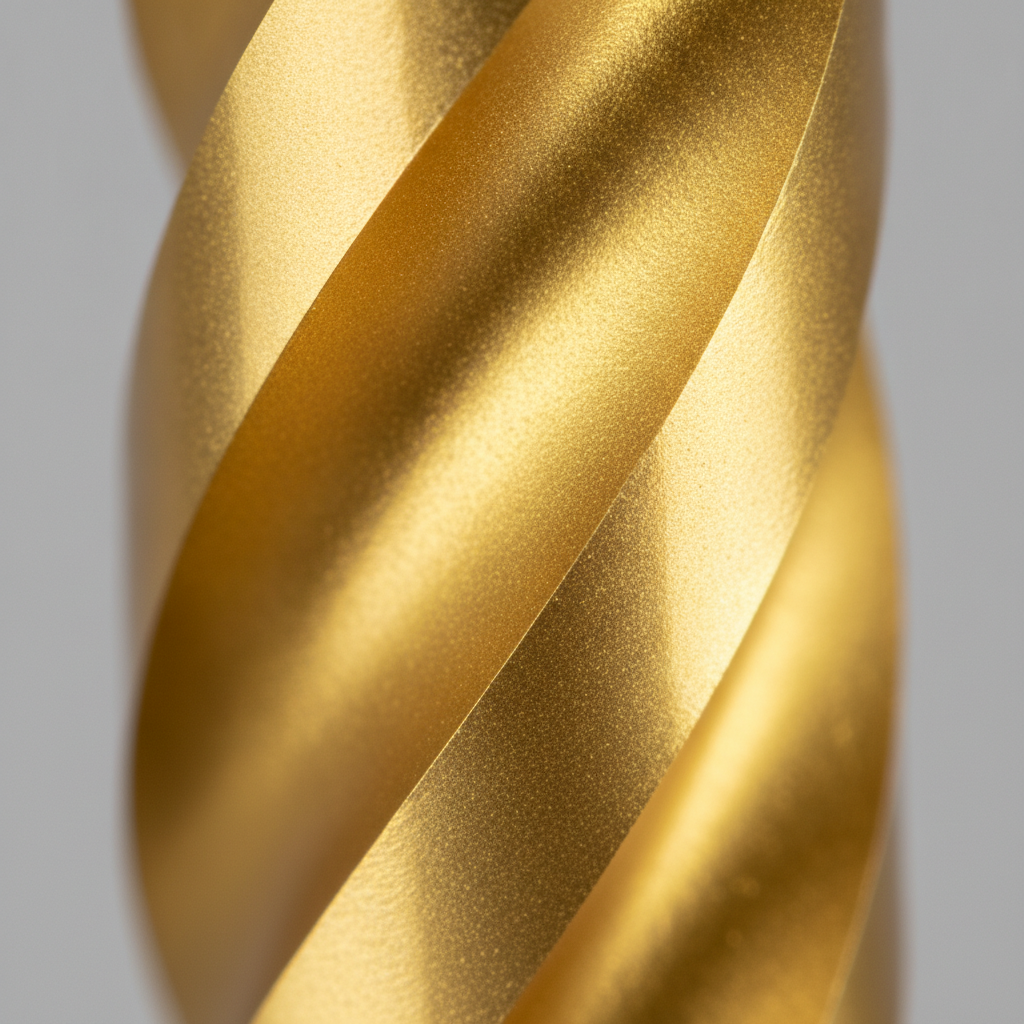
Vapor deposition coating is a family of thin-film processes that deposit hard, wear-resistant layers onto parts in vacuum or thermal spray environments. It boosts surface hardness, cuts friction, and improves corrosion resistance—key for manufacturers in Woodbridge running stamping, molding, or machining lines where uptime and tool life drive throughput.
By Sputtek • Last updated: 2026-07-01
Above-fold overview: why this guide matters
This practical guide explains vapor deposition coating in plain language for manufacturing teams. You’ll see how PVD and DLC work, when Thermospray/Pulsed HVOF is the better choice, and how to spec thickness, hardness, and prep. Real Woodbridge examples and checklists help you move from trial to stable production.
Use this page as your day-to-day field reference. We wrote it for engineers, toolmakers, and operations leaders who need fast, accurate answers without fluff.
- What vapor deposition coating is and how it works (PVD, DLC, Thermospray)
- When coatings beat base-material upgrades for wear, friction, and corrosion
- How to design for coating: edge radii, surface prep, masking, and QC
- Woodbridge-specific considerations and scheduling tips
- Actionable specs: temperature (150–500 °C), thickness (1–5 μm), hardness (up to ~3,000 HV)
What is vapor deposition coating?
Vapor deposition coating refers to depositing solid films from a vapor phase onto a substrate to improve surface performance. In practice, manufacturers use Physical Vapor Deposition (PVD), DLC (a carbon-based PVD family), and thermal spray methods to add hardness, lower friction, and resist wear and corrosion at thicknesses typically between 1–50 microns.
In our experience supporting high-volume programs, three approaches cover most needs:
- Physical Vapor Deposition (PVD): Evaporates or sputters metals/ceramics in vacuum and condenses them as a dense thin film. Typical thickness 1–5 μm, microhardness often 1,500–3,000 HV, and application temperatures around 150–500 °C.
- DLC coatings: Diamond-like carbon variants (e.g., a-C:H) deposited in vacuum, delivering low friction (as low as ~0.1–0.2 against steel) and high hardness while preserving sharp edges on cutting tools and precision components.
- Thermospray / Pulsed HVOF: Accelerates particles in a high-energy stream to build thicker layers (50–500+ μm). Ideal when you need robust build-up, corrosion barriers, or dimensional restoration beyond thin films.
Vapor deposition coating is central to the broader Deposition topic—and we explore fundamentals and applications deeply in our PVD deposition guide for reference continuity.
Why vapor deposition coating matters for manufacturers
Coatings unlock measurable productivity. Thin films lower friction by 20–60%, increase surface hardness into the 1,500–3,000 HV range, and stabilize part quality across thousands to millions of cycles. The result: fewer stoppages, steadier Cp/Cpk, easier release in molds, and longer intervals between regrinds or tool changes.
Here’s why teams in stamping, molding, machining, and component assembly specify coatings over base-alloy upgrades:
- Life extension without retooling: Adding 2–4 μm TiN, TiCN, AlTiN, or DLC onto existing tools often doubles usable life before wear hits tolerance limits.
- Lower friction, cleaner release: DLC friction coefficients ~0.1–0.2 reduce sticking and galling; in injection molds this often means faster fill/pack and less scuffing on high-gloss finishes.
- Thermal and chemical stability: Modern PVD films perform up to 800–900 °F service temperatures depending on chemistry; aluminum- and chromium-based films resist oxidation better than conventional tool steels.
- Better first-pass yield: More stable surfaces help hold dimension and finish, improving FPY and reducing unplanned downtime tied to tool repair or polish.
When you’re mapping improvements across a cell, it’s common to see coating-driven changes ripple into OEE: longer mean time between interventions, lower scrap percentage, and steadier cycle times across 10,000–100,000+ cycles.
For more fundamentals and vocabulary, see our quick primer on PVD plating basics and this adjacent explainer on PVD finishing that details post-coat lapping down to ~0.02–0.05 μm Ra surfaces.
Local considerations for Woodbridge
- Schedule high-volume batches to coincide with nearby logistics windows around SmartCentres Woodbridge freight carriers; consolidating loads reduces handling time between prep, coating, and return.
- Plan heat-sensitive work (polymer tooling, tempered edges) in shoulder seasons; humidity swings can affect incoming cleanliness—tighten degreasing checks April–June and September–October.
- Masking and inspection drop-offs near Weston Rd / Highway 7 are quick, but coordinate fixture returns if you’re cycling tools weekly to keep takt time stable.
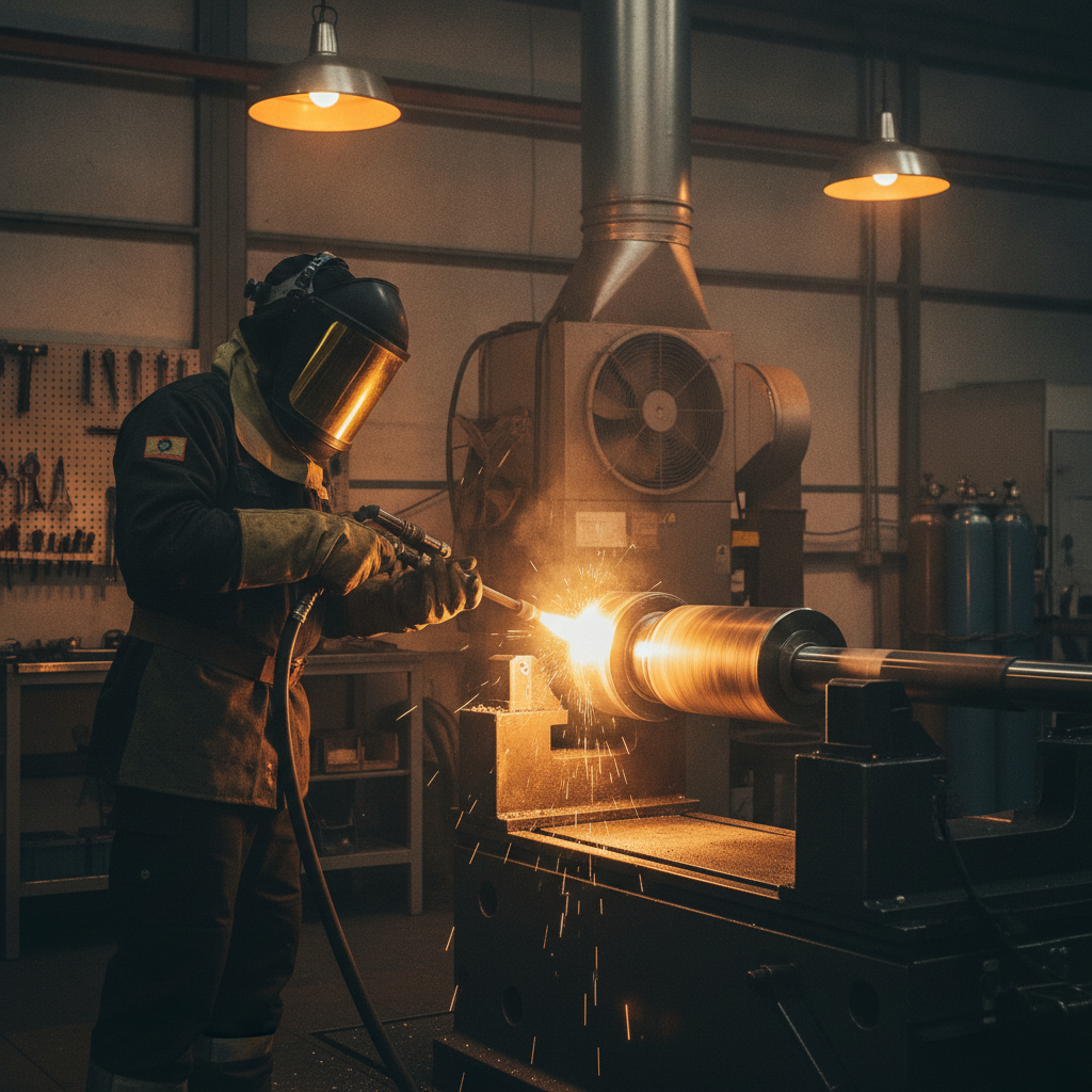
How PVD works: the step-by-step you can trust
PVD forms films by vaporizing source material in vacuum and condensing it on the part. Success depends on surface prep (Ra, degreasing), fixture orientation, vapor energy, and post-coat finishing. Expect chamber pressures around 10⁻³–10⁻⁶ Torr, temperatures near 150–500 °C, and deposition rates measured in nm/s.
- Preparation: Degreasing, ultrasonic cleaning, and microblasting achieve target roughness (often 0.1–0.4 μm Ra) and activate the surface. Edge prep (e.g., 10–30 μm hone) reduces stress concentrations.
- Masking & fixturing: Critical surfaces are masked; parts are oriented to ensure line-of-sight deposition. Rotation speeds are tuned to even out thickness within ±10–15% on complex geometries.
- Vacuum & plasma ignition: Chambers pull down to 10⁻³–10⁻⁶ Torr; plasmas sputter or evaporate source targets (Ti, Cr, Al, C) that condense atom-by-atom onto the substrate.
- Adhesion control: Ion etching and graded interlayers (e.g., Cr/CrN) boost adhesion; substrate temperature is managed to avoid softening or temper loss.
- Post-processing: Lapping and polishing return functional surfaces to spec, often to 0.02–0.05 μm Ra on optical or mirror-critical molds.
We outline additional thin-film concepts and terminology in our metal vapor deposition overview, which connects directly to fixturing and cycle planning.
Types, methods, and approaches you can deploy
Most programs benefit from three families: arc-PVD and sputter-PVD for thin, hard films; DLC variants for ultra-low friction; and Thermospray/Pulsed HVOF for thicker build-ups. Selecting among them hinges on temperature limits, needed thickness (1–500+ μm), edge retention, and required corrosion or oxidation resistance.
Common films and where they shine
- TiN (gold): General-purpose wear layer for steels and carbides; 1.5–3.0 μm typical, ~2,000 HV, good for stamping and basic cutting.
- TiCN: Harder than TiN and lower friction; often 2–4 μm; popular on punches, forming tools, and high-speed cutters.
- AlTiN / AlCrN: Higher hot-hardness and oxidation resistance; useful above ~900 °F service, e.g., dry milling or die-casting trim.
- DLC (a-C:H, ta-C): CoF ~0.1–0.2 on steel pairs, great release on plastics; often 1–3 μm; favors sharp-edge retention on small tools.
- Thermospray / Pulsed HVOF: 50–500+ μm thickness, corrosion/wear barriers on shafts, rolls, and sealing surfaces; supports dimensional restoration.
Comparison at a glance
| Method | Typical thickness | Process temp | Standout trait | Use cases |
|---|---|---|---|---|
| PVD (sputter/arc) | 1–5 μm | 150–500 °C | Hard, thin, edge-true | Stamping, molds, cutting tools |
| DLC (PVD family) | 1–3 μm | 150–350 °C | Ultra-low friction | Plastic molds, sliding pairs |
| Thermospray / Pulsed HVOF | 50–500+ μm | Ambient at substrate | Thick build, repair | Shafts, rolls, corrosion barriers |
| CVD (reference) | 5–20 μm | 800–1,000+ °C | Conformal coverage | High-temp ceramics/carbides |
For a fast refresher on terms used across this Deposition cluster, our thin films explainer for Woodbridge maps language to shop-floor decisions.
Best practices: design, prep, and production handoffs
Great coatings start well before the chamber. Specify edge radii, surface roughness, masking lines, and datum handling in your drawings. Standardize cleaning and incoming inspection. Align coating thickness (1–5 μm for PVD, 50–500+ μm for thermospray) to tolerance stacks and downstream finishing plans.
Design-for-coating checklist
- Edge conditioning: Hone cutting edges 10–30 μm for robustness; keep functional corners sharp where needed—DLC preserves geometry well at ~1–3 μm.
- Surface roughness: Aim for 0.1–0.4 μm Ra before PVD; polish critical optical or mold faces further if you need <0.05 μm Ra post-coat.
- Masking strategy: Call out no-coat fits, threads, and grounding points; provide masking sketches with ±0.2 mm tolerances on edges.
- Base material hardness: For HRC 58–64 tool steels or cemented carbides, PVD shines; for softer substrates needing build-up, consider thermospray.
- Tolerance stack: Allocate 1–5 μm for PVD plus any post-lap removal (often 0.2–0.5 μm) so assembled fits remain in spec.
Process control notes
- Cleanliness: A single fingerprint can ruin adhesion at 10⁻⁶ Torr; standardize solvent and ultrasonic cycles, then seal in dust-free containers.
- Fixturing density: Overcrowding can push thickness variation above ±15%; plan rack density to hit your Cp targets.
- Verification: Measure thickness (XRF), adhesion (scratch), hardness (microindentation), and friction when relevant; archive data per ISO 9001:2015.
- Post-coat finishing: Lapping stones, diamond paste, or vapor hone—select to reach Ra goals quickly without cutting through 1–3 μm DLC.
We codified these into a practical framework inside our best-practices finishing guide, built from dozens of start-ups we stabilized to daily-run status.
Tools, resources, and Sputtek capabilities
Sputtek’s in-house stack covers sandblasting, microblasting, cleaning, stripping, polishing, lapping, and QC—plus multiple PVD systems and a Thermospray cell. High-capacity SPUN PVD systems support ~1,200–3,000 kg/cycle, enabling prototype-to-volume scaling without quality drift.
- PVD systems: SPUN 2,000 (up to ~1,200 kg/cycle) and SPUN 4,000 (~3,000 kg/cycle) for large or dense batches; stable recipes across TiN, TiCN, AlTiN, AlCrN, and DLC families.
- Thermospray / Pulsed HVOF: Build thickness 50–500+ μm rapidly; restore worn shafts/rolls and add corrosion barriers while controlling heat input.
- Quality lab: XRF for thickness, scratch for adhesion, microhardness for HV, and optical surface metrology for Ra/Rz tracking.
- End-to-end: In-house degreasing, blasting, and lapping shrink total lead time by consolidating 3–5 vendor steps under one ISO 9001:2015 system.
If you’re mapping options, start with our complete DLC coating guide and the broader PVD deposition guide—they align terms with actionable tolerances and shop-floor checks.
Case studies and real-world examples
Across stamping, molding, and machining, vapor deposition coating programs often stabilize within one to two cycles of optimization. Common specs land at 1–4 μm thickness, Ra under 0.05–0.2 μm after lapping, and adhesion passing scratch thresholds—enough to shift OEE in sustained production runs.
Stamping dies: form tools and punches
A Tier-1 automotive stamper near Woodbridge used AlCrN at ~3 μm on AHSS form tools with a 20 μm edge hone. The line held dimension past 100,000 hits with visibly reduced galling, and regrind intervals aligned to planned PM windows. Surface Ra stabilized around 0.1–0.2 μm post-lap.
Plastic injection molds: high-gloss, easy release
For cosmetics packaging, we applied DLC at ~2 μm on mirror-finish cores and cavities. Friction dropped to near 0.1 on steel-plastic contact, improving release and reducing scuffing on Class-A surfaces. After-coat polishing returned faces to <0.03 μm Ra without breaking through the film.
Cutting tools: carbide end mills and drills
Carbide tools coated with AlTiN at ~2–3 μm retained sharp edges, supported dry milling regimes above 900 °F, and kept flank wear bands narrow across multi-hour runs. Shops reported steadier chip evacuation and predictable tool change intervals that matched SPC planning.
For additional PVD fundamentals that pair with these examples, our PVD plating overview and metal vapor deposition guide dive deeper into thickness control and adhesion mechanisms.
When to choose Thermospray (Pulsed HVOF)
Use Thermospray when you need thicker coatings, corrosion protection, or dimensional restoration. If the target is 50–500+ μm and heat input to the substrate must be minimal, Pulsed HVOF builds dense layers quickly while preserving base material properties and geometry.
- Repair and build-up: Bring shafts and rolls back to size with 100–300 μm coatings, then grind to tolerance.
- Barrier layers: Apply corrosion- and wear-resistant materials in a single pass strategy; porosity control and sealants further improve performance.
- Thermal management: Keep substrate temperatures low to avoid temper draw or distortion on long, slender components.
We coordinate thermospray schedules and QC alongside PVD work so you can keep a single traveler for prep, coat, grind, and inspect. For context on thermal equipment ecosystems, review common thermal process components used in industrial shops.
Specs and QA: the numbers that matter
Specify only what you need to control: thickness (μm), hardness (HV), roughness (Ra), adhesion (critical load), and masked areas. Typical PVD targets are 1–5 μm, 1,500–3,000 HV, and 0.02–0.2 μm Ra after lapping. DLC often delivers CoF ~0.1–0.2 against steel pairs.
- Thickness: 1–5 μm for PVD; 50–500+ μm for thermospray. Hold ±10–15% on complex geometries with smart fixturing.
- Hardness (HV): TiN ~2,000 HV; AlTiN/AlCrN can exceed 3,000 HV; many DLCs sit 2,000–4,000 HV microhardness.
- Friction (CoF): DLC ~0.1–0.2; TiN/TiCN typically higher; pair selection matters (steel vs aluminum vs polymers).
- Adhesion: Scratch test critical loads documented per your internal spec; include acceptance bands and retest logic.
- Roughness: Post-coat Ra 0.02–0.2 μm depending on function; confirm before assembly to avoid transfer marks.
If you work closely with polymers, this background on thermoplastics versus thermosets and general polymer selection context can help frame mold-release behavior when you’re deciding between hard nitrides and DLC.
Frequently Asked Questions
These short, direct answers cover the questions we hear most from Woodbridge manufacturers. Each response assumes production realities: limited downtime, tolerance stacks in microns, and the need to stabilize lines within one to two coating cycles.
What’s the difference between PVD and DLC?
PVD is the vacuum process that deposits many films (TiN, AlTiN, CrN, etc.). DLC is a specific family of carbon-based films within that toolkit. Choose DLC when you need very low friction (~0.1–0.2) and good edge retention; choose nitrides/oxides when hot hardness and oxidation resistance dominate.
How thick should my coating be?
For PVD, 1–5 μm covers most tools and molds while preserving geometry and sharp edges. For repair or barrier needs, Thermospray/Pulsed HVOF typically lands between 50–500+ μm, followed by grinding or polishing to final dimension and surface finish.
Will PVD change my part dimensions?
Yes, by the thickness you specify. A 3 μm film adds ~6 μm to a diameter. Account for this in tolerance stacks and note any post-lapping removal (often 0.2–0.5 μm) on critical faces before assembly.
How fast can we stabilize a coating program?
Most lines stabilize within one or two coating cycles once you define prep, thickness, and finishing. Document Ra targets, edge hones (10–30 μm), and fixture orientation to keep thickness within ±10–15% and reduce trial loops.
Key takeaways
Match the method to the job: thin, hard PVD/DLC for precision tools and molds; thicker Thermospray for repair and barriers. Control prep, thickness, and finishing, and you’ll see stability within one to two cycles and measurable gains in uptime and part quality.
- Vapor deposition coating is your lever for hardness (1,500–3,000 HV), friction (~0.1–0.2 with DLC), and reliable release.
- Specify 1–5 μm for PVD, plan for post-lapping removal, and document acceptance tests (XRF, scratch, microhardness).
- Use Pulsed HVOF when you need 50–500+ μm build-ups or corrosion barriers with minimal heat input.
- Standardize drawings: edge hone, Ra, masking, and datum handling keep lines stable and SPC clean.
Conclusion: move from trials to stable production
If you control prep, thickness, and finishing, vapor deposition coating quickly becomes a repeatable, high-yield step in your production flow. Start small, verify adhesion and Ra, then scale batch density once thickness variation is within ±10–15% on your geometry.
Ready to translate specs into a production-ready coating? Explore our metal vapor deposition overview and bookmark the PVD deposition guide for deeper dives on fixturing, adhesion stacks, and post-coat finishing.
Prefer a quick consult? Our Woodbridge team can review a print and recommend a PVD film (1–5 μm) or a Thermospray build (50–500+ μm) plus a finishing plan. Let’s make your line steadier, cycle by cycle.


