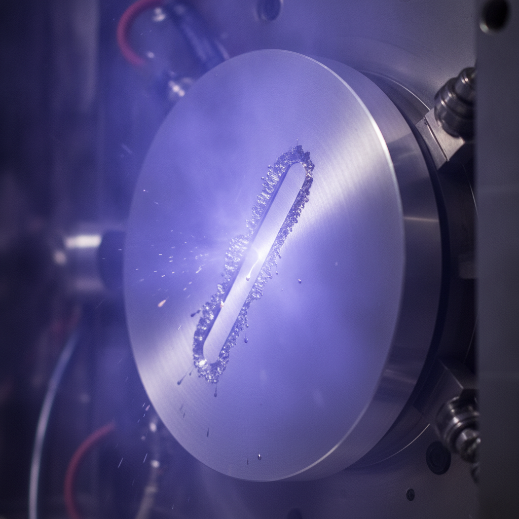
Physical vapor deposition sputtering is a vacuum thin‑film process that ejects atoms from a target and deposits them on a substrate to form a durable coating. It delivers dense, well‑adhered films for wear, friction, and corrosion control. From our facility at 110 Sharer Rd in Woodbridge, we apply PVD sputtering to engineer longer tool life and steadier throughput.
By Ron — Sputtek
Last updated: 2026-06-13
Above‑Fold Guide and Quick TOC
This complete guide explains PVD sputtering in plain terms, when to use it, and how to get repeatable results. You’ll learn core physics, process steps, equipment options, QA checks, and real examples from high‑demand manufacturing. Use the table of contents below to jump to what you need now.
- What is PVD sputtering?
- At a Glance: Summary
- Why it matters for manufacturing
- How sputtering works (step‑by‑step)
- Types and methods
- PVD sputtering vs alternatives
- Best practices
- Tools, materials, and resources
- Case studies and examples
- FAQ
- Key takeaways
- Conclusion and next steps
At a Glance: Summary
PVD sputtering creates thin, functional films by transferring atoms from a solid target to a workpiece under vacuum. Choose it for adhesion, uniformity on complex shapes, and tight control of film stress and composition—especially when you want to improve performance without changing the base part.
- What it solves: Wear, galling, built‑up edge, corrosion, sticking in molds, inconsistent surface energy.
- Where it shines: Cutting tools, stamping dies, injection molds, and precision components.
- Film ranges: ~50 nm to ~5 μm; process pressure often 1–10 mTorr; baseline vacuum ~10−5 Torr.
- Industrial stacks: TiN, CrN, AlTiN, multilayers, and sputtered interlayers beneath DLC.
- Result: Longer tool life, steadier cycle time, and more consistent first‑pass yield.
For deeper background on deposition choices, see our internal primer on PVD coating fundamentals and this rundown of deposition types used in industry.
What Is Physical Vapor Deposition (PVD) Sputtering?
PVD sputtering is a plasma‑assisted vacuum process that knocks atoms from a target using energetic ions and deposits them as a thin film on nearby parts. It enables precise, dense coatings—like TiN, CrN, AlTiN, and DLC interlayers—on tools, dies, and components.
In practice, inert argon gas becomes an ionized plasma. Ions accelerate toward a negatively biased target (cathode), dislodging atoms that travel ballistically to the substrates. Those atoms condense to form a film with controllable composition and microstructure. Add reactive gases (e.g., nitrogen) to form compounds in‑situ.
- Key outputs: Hardness, lower friction, improved corrosion resistance, tuned optical/electrical properties.
- Common targets: Ti, Cr, AlTi, Zr, W, Mo, Si, C (graphite), plus alloys and ceramics.
- Typical thickness: 0.5–5 μm for wear; 50–500 nm for functional layers and diffusion barriers.
- Deposition rates: Often 0.1–5 μm/hour depending on power density, magnetron configuration, and geometry.
For manufacturers, the appeal is simple: you can transform the working surface without redesigning the base material. Coated tools last longer and run faster, stabilizing takt time and scrap rates in high‑volume lines.
To explore other PVD routes alongside sputtering, skim our guide to PVD methods that compares arc, evaporation, and hybrid stacks.
Why PVD Sputtering Matters
Sputtered films increase uptime, improve yield, and standardize quality by reducing wear, friction, and built‑up edge. That’s why automotive, aerospace, medical, and energy manufacturers integrate sputtering into their process control plans.
- Tool life extension: AlTiN and CrN films on cutting tools resist oxidation and crater wear at elevated temperatures.
- Surface energy control: Coatings on injection molds reduce sticking and flow hesitation, stabilizing cycle time.
- Corrosion/diffusion barriers: Multilayers and nitrides isolate base metals from aggressive chemistries.
- Dimensional stability: Micron‑scale films preserve tolerances on precision components and mating features.
- Traceability: Characterizable films (hardness, thickness, roughness) support PPAP and regulatory documentation.
Across production lines, even single‑digit percentage gains in uptime can yield thousands more good parts per week. Coatings are one of the few levers that materially change wear and friction while leaving the design intact.
When friction is the constraint, DLC stacks are powerful. For the fundamentals and where DLC fits, see our complete DLC coating guide.
How PVD Sputtering Works (Step‑by‑Step)
Sputtering follows a disciplined sequence: prepare surfaces, load and fixture, evacuate and heat, ignite plasma, deposit, cool, and verify. Each step has measurable controls that drive adhesion, density, and uniformity.
- Clean and prep: Degrease, ultrasonic clean, microblast, and activate surfaces. Ra, Rz, and burr control influence adhesion.
- Mask and fixture: Use shadow masks and rotation/planetary motion to target coverage and control thickness.
- Vacuum and heat: Pump down to ~10−5 Torr baseline; heat to drive off volatiles and reduce water layers.
- Etch: Argon plasma etching and bias clean remove residual oxides and improve nucleation.
- Deposit: Strike plasma at the target; maintain power, pressure (often 1–10 mTorr), and gas flows. Add nitrogen/acetylene for reactive films.
- Cool under vacuum: Prevent oxidation and moisture adsorption; stabilize stresses.
- Validate: Measure thickness, hardness, and adhesion; document lot conformance.
Process windows are defined by power density, pressure, substrate bias, and temperature. Small drifts in these variables show up as thickness variation, stress changes, or phase shifts—so closed‑loop control pays off in day‑to‑day production.
Actionable controls you can set today
- Surface finish targets: For wear coatings, finish to low Ra after lapping; too rough increases friction and accelerates wear.
- Edge prep: Micro‑chamfer sharp edges (e.g., 0.02–0.05 mm) to reduce stress and flaking under load.
- Recipe discipline: Version‑control power, pressure, gas flows, bias, and temperature; lock change approval.
- Target conditioning: Pre‑sputter to stabilize rates and cut particles before exposing parts.
- Lot metrology: Check thickness (XRF or calotest), roughness (Ra/Rz), and adhesion (Rockwell/scratch) every batch.
For a broader context on PVD process choices, compare these steps with the approaches in our overview of PVD methods.
Types and Methods of Sputter Deposition
Different sputter methods trade rate, energy, and coverage. DC magnetron is the workhorse for metals; RF handles dielectrics; reactive sputtering forms nitrides; HIPIMS boosts ionization for dense films and strong adhesion.
Core methods
- DC magnetron sputtering: Efficient metal removal with racetrack erosion; great for TiN, CrN, and alloy layers.
- RF sputtering (13.56 MHz): Deposits insulators and semiconductors; useful for oxides and barrier layers.
- Reactive sputtering: Introduce N2, O2, or C‑containing gases to form compounds at the substrate.
- HIPIMS/HiPIMS: High‑power pulses increase ionization, improving film density and step coverage on complex parts.
- Co‑sputtering: Two or more targets run simultaneously to tailor composition or create graded layers.
Geometry and motion
- Confocal magnetrons: Multiple guns aimed at a rotating fixture for uniformity on 3D parts.
- Planetary motion: Part carriers spin while orbiting; averages angular effects and evens thickness.
- Line‑of‑sight masking: Manage shadowed features; design for venting and no trapped volumes.
Method selection is driven by substrate temperature limits, desired phase (e.g., AlTiN vs TiAlN), and throughput targets. For DLC stacks, chromium or silicon interlayers via sputtering can anchor adhesion before the carbon topcoat.
For a structured deep dive into PVD options, check our PVD types comparison.
PVD Sputtering vs. Alternatives
Choose sputtering for uniform, dense films on temperature‑sensitive parts; choose arc PVD for ultra‑hard nitrides at higher energy; pick evaporation for simple line‑of‑sight coatings; select HVOF/Thermospray when you need 50–300 μm thick build‑up.
| Method | Typical Thickness | Adhesion/Density | Conformality | Heat to Part | Use Case |
|---|---|---|---|---|---|
| Sputtering (PVD) | 0.05–5 μm | High/High | Good on 3D | Low–Moderate | Tools, molds, barriers |
| Arc PVD | 1–5 μm | Very High/High | Moderate | Moderate–High | Ultra‑hard nitrides |
| Evaporation (PVD) | 0.05–2 μm | Moderate/Moderate | Line‑of‑sight | Low | Optical/reflective films |
| HVOF/Thermospray | 50–300 μm | Mechanical bond | Bulk build‑up | High (localized) | Erosion/corrosion layers |
Hybrid stacks are common. A sputtered adhesion layer can sit under an arc‑grown nitride or a DLC film to combine benefits—bond strength from sputtering, extreme hardness or low friction from the top layer. For thicker rebuilds or erosion control, our Thermospray (Pulsed HVOF) cell addresses 50–300 μm applications.
Best Practices for Repeatable Results
Consistency comes from surfaces, fixturing, and controls. Nail cleanliness, geometry, and set points; then verify with metrology. That’s the formula for coating performance that holds up in production.
Surface and geometry
- Finish for function: For wear coatings, aim for low Ra after lapping; excessive roughness increases friction.
- Radius edges: Sharp edges concentrate stress; micro‑chamfers improve film integrity under load.
- Match mask to motion: Design masks around rotation and line‑of‑sight to avoid thin spots.
- Degreasing discipline: Oils trapped in blind holes will outgas; design for cleaning and venting.
Process control
- Document recipes: Power, pressure, gas flows, bias, and temperature should be controlled with MOC discipline.
- Warm‑up and conditioning: Pre‑sputter targets to stabilize rate and reduce particles before exposing parts.
- Lot‑level metrology: Cross‑section thickness, nanoindentation hardness, adhesion (Rockwell/Calo), and roughness checks.
- Bias tuning: Use substrate bias to manage stress and density; track via curvature or XRD where applicable.
Quality and documentation
- Traceability: Tie each rack to batch IDs and instrument logs; align with PPAP or device history record needs.
- Risk overlays: Use FMEA to catch geometry, masking, and motion issues before the first article.
- Production DOE: A short fractional DOE reveals the most sensitive parameters for your geometry and alloy.
In our experience at Sputtek, 80–90% of repeatability issues trace back to prep, fixturing, or subtle parameter drift. Tighten those three and your process window widens noticeably.
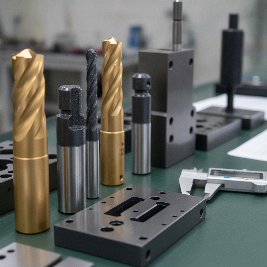
Tools, Materials, and Resources
In Woodbridge, within the Regional Municipality of York, we combine high‑capacity PVD platforms, robust fixturing, and disciplined QA to turn recipes into stable production. System design, target purity, and metrology are the levers that keep runs consistent.
- System platforms: Batch PVD systems with multiple magnetrons, rotation/planetary motion, and substrate bias control.
- Targets and gases: High‑purity targets; argon for plasma; nitrogen/acetylene/oxygen for reactive films.
- Fixturing: Racks that minimize shadows and ensure even exposure to each cathode.
- Metrology: XRF or calotest for thickness; nanoindentation; optical profilometry; scratch or Rockwell adhesion mapping.
- Documentation: Controlled recipes, lot travelers, and instrument calibration records.
Local considerations for Woodbridge
- Schedule pickups and deliveries to avoid peak traffic near Weston Rd / Highway 7; it helps time‑sensitive changeovers.
- Winter humidity swings affect storage; keep fixtures and cleaned parts sealed when moving to and from SmartCentres Woodbridge area.
- For onsite trials at 110 Sharer Rd, align runs with your maintenance windows to validate cycle time impact the same week.
Our SPUN series PVD systems are built for scale. SPUN 2,000 supports heavy racks; SPUN 4,000 handles up to multi‑thousand‑kilogram cycles—ideal for large stamping dies and extrusion tooling. Pairing the right target set with rotation schemes can trim thickness variation to within a few percent on 3D parts.
For background on how material purity and process discipline influence coatings, see this discussion of custom polymer synthesis fundamentals and a practical process control checklist. The principles—purity, repeatability, and documentation—parallel what we enforce in sputtering.
Case Studies and Examples
Real manufacturing wins come from matching coating stack, geometry, and duty cycle. Here are brief examples that mirror common production problems—and how sputtering helps solve them.
- Stamping dies (automotive): Nitrides on forming surfaces cut galling and reduce downtime between die maintenance cycles. We’ve seen interval extensions from a few thousand to tens of thousands of hits before re‑polish when stacks and prep align.
- Injection molds (plastic processing): Low‑energy films and polished cavities reduce sticking and shorten cooling phases. Even a 3–5% cycle time improvement compounds across multi‑cavity tools and shifts.
- Cutting tools (machining): AlTiN over a Cr interlayer stabilizes crater wear at high surface speed with dry‑cut conditions. Shop‑floor metrics often show steadier surface finish across the tool’s lifespan.
- Aluminum die cast/extrusion: Multilayer stacks combat soldering and die erosion, preserving surface finish and dimensions across extended runs.
- Pharma tooling: Hard, low‑roughness coatings on punches extend life and support consistent tablet weight and finish under repetitive loads.
Each scenario starts the same way: define failure modes, measure baseline life, and run a controlled trial. When the stack and recipe match the duty cycle, double‑digit improvements in tool life and steadier Cp/Cpk are common.
How we operationalize success at Sputtek
- Certifications that matter: ISO 9001:2015 and Nuclear N299.3 support regulated programs and documentation rigor.
- End‑to‑end workflow: In‑house sandblasting, microblasting, degreasing, stripping, polishing, lapping, and QC lab reduce handoffs and lead‑time risk.
- Scale without chaos: High‑capacity SPUN systems (multi‑thousand‑kilogram cycles) keep large batches consistent rack‑to‑rack.
Want the broader landscape beyond sputtering? Our high‑performance coatings overview maps typical stacks to failure modes and applications.
Our engineering team in Woodbridge can review your tooling, propose a sputtered stack, and outline a validation plan that fits your production window.
Frequently Asked Questions
These short answers address the most common sputtering questions buyers ask during trials and ramp‑up. They’re designed for quick quoting and process planning.
What is the main advantage of PVD sputtering over evaporation?
Sputtering offers denser films and better adhesion on complex shapes. It also supports reactive compounds like TiN or CrN with good uniformity. Evaporation is fast and simple for line-of-sight coatings, but it’s less conformal and generally has lower film density.
Can PVD sputtering handle temperature‑sensitive substrates?
Yes. Sputtering typically runs at lower substrate temperatures than arc PVD and far below thermal spray, making it suitable for many steels, some aluminum alloys, and polymer tooling inserts when properly fixtured and cooled.
Which coatings are most common for wear resistance?
TiN, CrN, AlTiN, and multilayers are common for tools and dies. A sputtered interlayer often anchors a DLC topcoat where very low friction is needed. The right choice depends on heat, load, and the material you’re cutting or forming.
How do you verify coating adhesion?
We combine scratch or Rockwell indentation with cross-section inspection and lot-level thickness checks. Adhesion also shows up in field performance—edge retention, crater wear, and resistance to flaking during cleaning cycles.
Is physical vapor deposition sputtering compatible with DLC?
Yes. We commonly sputter chromium or silicon interlayers to anchor DLC stacks. This combination delivers strong adhesion plus very low friction, which is ideal for sliding contact, sealing, and certain mold release scenarios.
Key Takeaways
Sputtering delivers dense, adherent thin films with strong control over composition and stress—ideal for tools, molds, and critical components. The best results come from disciplined prep, fixturing, and closed‑loop recipes.
- Physical vapor deposition sputtering balances adhesion, density, and conformality for complex parts.
- Surface prep and motion design largely determine real‑world performance.
- Metrology closes the loop—measure thickness, hardness, and adhesion by lot.
- Use reactive and multilayer stacks to tune wear, friction, and corrosion.
- Leverage Sputtek’s ISO and nuclear approvals when documentation rigor is essential.
Conclusion and Next Steps
If you’re targeting longer tool life and steadier cycle time, sputtering is a high‑leverage upgrade. Define failure modes, lock in prep and fixturing, then validate with a small DOE before scaling.
At Sputtek’s Woodbridge facility, we combine PVD sputtering, DLC stacks, and Thermospray (Pulsed HVOF) to match technology to the job. When you’re ready, we’ll propose a coating stack, fixture plan, and QA routine aligned to your production goals—and document it to your PPAP or device record requirements.
For readers building internal SOPs, these primers on process design discipline echo the same manufacturing truths: define inputs, control variables, and verify outputs—exactly how robust sputtering is run.


