Physical vapor deposition is a vacuum coating process that deposits thin, hard films such as TiN, AlTiN, and DLC onto tools and components to reduce wear and friction. At Sputtek’s facility at 110 Sharer Rd in Woodbridge, we apply PVD and related coatings across prototypes and high‑volume runs to extend tool life and stabilize production quality.
By Ron — Sputtek
Last updated: 2026-06-10
At a Glance
PVD creates dense, adherent coatings in a vacuum by vaporizing solid materials and condensing them on parts. For manufacturers, the result is higher wear resistance, lower friction, and more predictable cycles. This guide explains what PVD is, how it works, where it wins, and how Sputtek implements it end‑to‑end.
Use this overview to decide where physical vapor deposition fits your tooling and component strategy, and how to partner with a certified provider that can scale from trial to production without surprises.
- What PVD is and why it matters for uptime and quality
- How sputtering, arc, HiPIMS, and DLC deposition differ
- Where PVD outperforms CVD, HVOF/Thermospray, and nitriding
- Actionable prep, masking, and QC steps that cut rework
- Real examples from stamping, plastic injection, and machining
For deeper dives on variants and finishes, see our in‑cluster primer on PVD coating types.
What Is Physical Vapor Deposition (PVD)?
Physical vapor deposition (PVD) is a family of vacuum processes that convert solid coating materials into vapor and condense them onto parts as thin, hard films. Typical layers range from microns to tens of microns and deliver wear resistance, low friction, and oxidation control for demanding industrial applications.
In practice, PVD is a controlled vacuum environment where target materials (for example, titanium or carbon sources) are energized to release atoms or ions. Those species travel through the chamber and nucleate on clean, prepared surfaces, building dense films with engineered phases and stoichiometry. Because PVD occurs at relatively moderate substrate temperatures compared with diffusion processes, it preserves base material properties and dimensions—critical for precision tooling.
- Common outputs: TiN, TiCN, AlTiN, CrN, ZrN, and DLC variants
- Typical thickness: ~1–5 µm on cutting tools; 2–10+ µm on dies/components
- Primary benefits: 2–10× reported tool life, tighter dimensional stability, smoother running
At Sputtek, PVD is paired with disciplined pre‑ and post‑processing—microblasting, cleaning, fixturing, and lapping—to turn coating performance into predictable production results.
Why PVD Matters to Manufacturers
PVD boosts throughput and quality by slowing abrasive wear, reducing galling, and moderating heat. Teams often see fewer changeovers, more consistent first‑pass yield, and stabilized Cpk when PVD is matched to the job, substrate, and finish target.
When uptime drives margin, every avoidable changeover hurts. A well‑specified PVD stack balances hardness, toughness, and lubricity so tools cut cooler and surfaces release cleanly.
- Fewer unplanned stops: Many shops report 20–40% fewer tool change events after dialing in the right PVD and edge prep.
- Lower scrap: A more stable friction coefficient can pull part‑to‑part variation down, supporting higher first‑pass yield.
- Thermal control: Heat at the chip/tool or part/mold interface drops when coatings reduce adhesion and rubbing.
- Cleanability: Dense, inert films release residues faster, cutting downtime between batches.
Because PVD runs at moderate substrate temperatures, it protects sharp edges and base microstructures that high‑temperature processes can soften. That’s a big reason it’s favored on carbide tools, stamping dies, and precision molds.
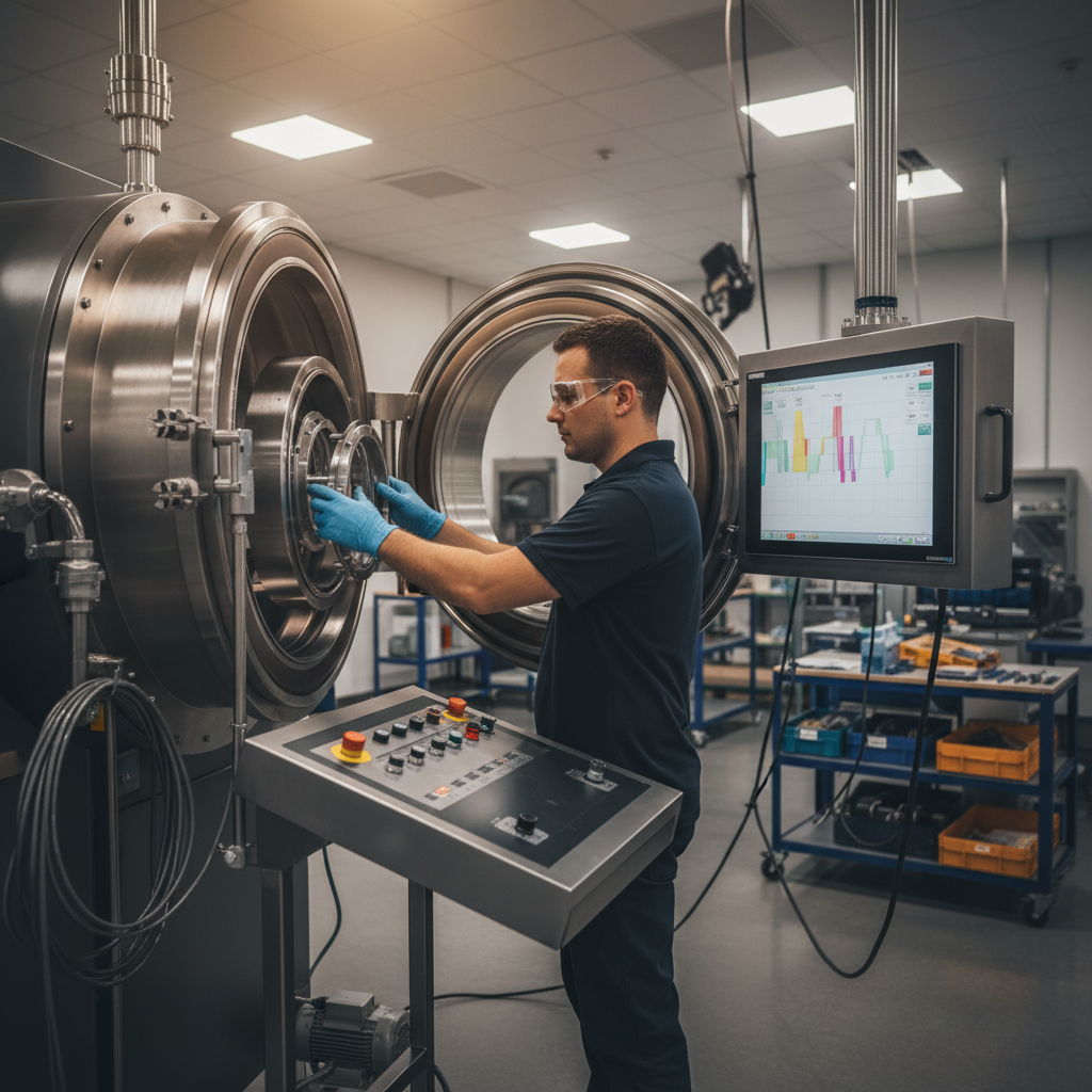
How Physical Vapor Deposition Works
PVD energizes a solid target inside a vacuum chamber, ejecting atoms or ions that travel to fixtured parts and condense into a thin film. Control of vacuum, power, bias, temperature, and gas chemistry tunes adhesion, hardness, stress, and friction behavior for the job.
Here’s a practical run‑down of a typical PVD cycle as we execute it in our Woodbridge facility.
- Intake and documentation: We capture alloy, hardness, prior treatments, drawing tolerances, and surface Ra/Rz targets. Clear inputs prevent over‑coating or unintended diffusion.
- Pre‑treatment: In‑house sandblasting or microblasting sets anchor patterns when needed; precision degreasing removes machining residues. Cleanliness is non‑negotiable.
- Masking and fixturing: Critical fits are masked; parts are oriented for uniform line‑of‑sight coverage. Good fixturing can swing thickness uniformity by double digits.
- Chamber conditioning: We pump down to high vacuum, stabilize temperature, and run burn‑in as needed to minimize contaminants.
- Deposition: Sputtering, cathodic arc, or HiPIMS sources release material; reactive gases (for example, nitrogen) form compound films like TiN or AlTiN.
- Bias and rotation: Substrate bias and multi‑axis rotation drive step coverage and film densification. This is where adhesion and texture are won or lost.
- Cool‑down and unload: Controlled cool‑down protects adhesion. We verify thickness and appearance before post‑process.
- Post‑process: Stripping and polishing or lapping fine‑tunes edge radii and bearing surfaces to spec.
- QC and release: We log thickness uniformity and adhesion checks, then release with traceable lot documentation.
In our experience, consistent inlet cleanliness and fixturing discipline eliminate most downstream headaches. If you perfect those two inputs, you avoid the majority of rework loops.

Types and Methods: Sputtering, Arc, HiPIMS, and DLC
PVD methods differ by how they eject material and build films. Sputtering yields smooth, dense layers; cathodic arc delivers high ionization and strong adhesion; HiPIMS combines sputter smoothness with arc‑like ion energy; DLC variants add ultra‑low friction and chemical inertness.
Choosing a method starts with the failure mode you’re solving—abrasive wear, adhesion, heat, or corrosion—and the substrate and geometry you’re coating.
Sputtering (DC, RF, Magnetron)
- What it is: Plasma knocks atoms from a target; they condense on parts. Magnetron sputter improves rate and film quality.
- Why it matters: Produces very smooth films—great for sliding, sealing, and cutting edge retention.
- Where we use it: Precision molds, sealing faces, and components needing tight Ra.
- Learn more: Our quick primer on PVD methods outlines selection trade‑offs.
Cathodic Arc
- What it is: A high‑current arc spot vaporizes cathode material, ejecting ions with high energy.
- Why it matters: Excellent adhesion and high density; modern filtering tames macroparticles for smoother finishes.
- Where we use it: Heavy‑duty tooling, forming dies, and wear faces that see impact and heat.
HiPIMS (High‑Power Impulse Magnetron Sputtering)
- What it is: Pulsed, very high‑power sputtering that increases ionization of the sputtered vapor.
- Why it matters: Arc‑like adhesion with sputter‑level smoothness; tunable stress and texture.
- Where we use it: Complex shapes, sharp cutting edges, and applications demanding uniformity.
DLC (Diamond‑Like Carbon) Families
- What it is: Amorphous carbon films with sp2/sp3 bonding; hydrogenated and hydrogen‑free variants exist.
- Why it matters: Very low friction and chemical inertness; useful against galling and sticky materials.
- Where we use it: Food and packaging blades, medical instruments, and sliding pairs.
- Deep dive: See our DLC coating guide for selection tips.
When in doubt, we start with the failure you’re trying to stop—alo ng with your cleaning window and target edge radius—then recommend a stack and method that’s both robust and maintainable.
PVD vs Alternatives: Quick Comparison
PVD excels when you need hard, thin, low‑friction films without altering base metallurgy. CVD suits high‑temperature, diffusion‑driven layers; HVOF/Thermospray builds thick, impact‑tough overlays; nitriding modifies the surface of steels for wear and fatigue strength.
Use this table to align process choice with geometry, heat budget, and failure modes.
| Process | Typical Thickness | Substrate Temp | Key Strength | Common Uses |
|---|---|---|---|---|
| PVD (sputter/arc/HiPIMS) | 1–10 µm | Low‑to‑moderate | Hard, low‑friction films; preserves base | Cutting tools, dies, molds, components |
| CVD | 5–15 µm | High | Conformal diffusion coatings | High‑temp wear/oxidation protection |
| HVOF/Thermospray | 50–500+ µm | Low‑to‑moderate | Thick, tough overlays | Shafts, rolls, corrosion/erosion faces |
| Nitriding | 10–200 µm (diffusion case) | Moderate | Surface hardening of steels | Gears, dies, fatigue improvement |
Sputtek offers both PVD and Thermospray (including Pulsed HVOF) in‑house, so you don’t have to choose blind. For material‑specific tips, see our notes on PVD coating types and deposition methods.
Best Practices That Prevent Rework
The fastest path to stable PVD performance is disciplined surface prep, smart masking/fixturing, and targeted post‑finishing. Get cleanliness right, control edge radii, and verify thickness/adhesion consistently—you’ll avoid most failure loops before they start.
From intake through release, here’s what consistently moves the needle in our lab and on our customers’ floors.
- Start with finish intent: Define the Ra/Rz you need after coating. This guides whether to lap or polish pre‑ or post‑coat.
- Specify critical fits: Mask bores, gauges, and sealed faces you can’t rework. Note allowable build‑up on non‑critical faces.
- Clean like it’s optics: Oil films and polishing compounds sabotage adhesion. Degrease and verify water‑break free surfaces.
- Edge discipline: Over‑sharp edges can chip; over‑heavy rounding dulls tools. Align edge prep with coating hardness and service.
- Fixture for flow: Position parts for even line‑of‑sight and rotation. Expect 10–20% swings in thickness from poor fixturing.
- Document and repeat: Record cycle parameters and results; small tweaks in bias or gas flow often yield measurable gains.
- Post‑process with intent: Light lapping can lower friction and bring a coated Ra back to spec without stripping.
We’ve found that simple incoming controls—cleanliness checks and a quick edge‑prep audit—drive outsized gains. For selection help, compare finishes in our types of PVD guide.
Free process assessment: Not sure if PVD, DLC, or Thermospray is the better path? Share a recent failure mode and we’ll map a trial plan that preserves fit/function and proves repeatability before you scale.
Tools and Resources
Successful PVD programs depend on clear specifications, repeatable fixturing, and measurable QC. Use the following resources—selection checklists, fixturing guides, and quality references—to keep trials tight and scale‑up predictable.
Bookmark these practical aids as you design or troubleshoot a coating program.
- Selection worksheet: Define substrate, finish target, contact mechanics, heat budget, and cleaning window.
- Fixturing checklist: Line‑of‑sight coverage, rotation paths, and shadow management.
- QC kit: Thickness, adhesion checks, and friction benchmarks; log before/after Ra for every batch.
- Automation inspiration: See examples of industrial coating automation to reduce handling risk.
- Purity mindset: Clean input matters more than clever parameters; note how labs approach high‑purity workflows to avoid contamination.
- Measurement thinking: While polymer‑specific, GPC methods illustrate tight quality control discipline that translates to coating labs.
Within our deposition cluster, we also maintain quick references on PVD methods and finish selection for common shop scenarios.
Case Studies and Practical Examples
Applying PVD well is about matching film chemistry and texture to real failure modes. These brief scenarios show how substrate, edge prep, and post‑finishing choices translate into measurable uptime and quality improvements on the floor.
Below are anonymized but representative situations we’ve supported in our 15,000 sq ft Woodbridge facility.
Stamping: AHSS Die Galling
- Problem: Advanced high‑strength steel panels were sticking, causing polish‑repair every shift.
- Approach: Arc‑grown TiCN with light post‑lap to target Ra, plus release‑agent cleaning SOP.
- Outcome: Unplanned polish events dropped by ~60%; panel cosmetics stabilized across runs.
Plastic Injection: Mold Venting and Release
- Problem: High‑fill glass‑fiber mix wore gate edges, flashing increased, vents fouled quickly.
- Approach: Smooth sputtered CrN on critical faces; DLC on sliding pairs; adjusted vent maintenance interval.
- Outcome: Gate edge retention improved; flashing complaints fell; vent cleaning extended by one shift on average.
Machining: Carbide End Mills in Heat‑Resistant Alloys
- Problem: Notching and BUE (built‑up edge) limited tool paths in nickel alloys.
- Approach: AlTiN via HiPIMS with bias tuning and controlled edge radius; documented tool‑set pairing.
- Outcome: 30–50% longer path length per tool reported; chatter decreased at target SFM.
Aluminum Die Cast / Extrusion: Soldering on Dies
- Problem: Aluminum soldering on die faces forced frequent downtime to strip residue.
- Approach: DLC variant tuned for lubricity; tighter cleaning standard between heats.
- Outcome: Release improved; downtime per shift down by a reported 20–30%.
Components: Corrosion and Sliding Wear
- Problem: Mixed corrosion and fretting on precision steel components in a moist environment.
- Approach: CrN base with carbon‑rich top layer; fixtured for uniform line‑of‑sight; post‑lap on bearing zones.
- Outcome: Visual corrosion complaints declined; wear marks minimized in teardowns.
These outcomes are repeatable because inputs are controlled: surface prep, orientation, rotation, and disciplined QC. That’s the backbone of Sputtek’s prototype‑to‑production approach.
Working with Sputtek in Woodbridge (Regional Municipality of York)
For teams in Woodbridge and the Regional Municipality of York, Sputtek offers local intake, rapid trials, and scale‑ready PVD/DLC and Thermospray. Our engineering‑led workflows and in‑house lab shorten the loop from failure analysis to stable coating recipes you can run at volume.
We’re Canada’s largest PVD/DLC service provider, operating multiple coating systems and a Thermospray cell. Proximity to neighborhood transit like Weston Rd / Highway 7 and retail hubs such as SmartCentres Woodbridge makes drop‑offs and pickups straightforward for local manufacturers.
Local considerations for Woodbridge
- Coordinate deliveries to avoid Highway 7 rush periods; we can stage parts to match your takt time and shift changes.
- Cold snaps and summer humidity can change handling; protect cleaned parts in sealed containers until chamber load.
- For quick drop‑ins, plan routes around Weston Rd / Highway 7; SmartCentres Woodbridge is a convenient waypoint for same‑day errands.
Frequently Asked Questions
These short answers address common PVD questions from engineering and operations teams. Each response is direct and practical so you can make fast, confident decisions about tooling, components, and trial planning.
What is the ideal thickness for PVD on cutting tools?
Most carbide cutting tools perform well around 2–5 microns, depending on edge radius and alloy. Thin enough to preserve sharpness; thick enough to resist abrasion and heat. Complex geometries or impact‑heavy service may justify slightly different targets after trial cuts.
How do I decide between PVD and Thermospray (HVOF)?
Pick PVD when you need a thin, hard, low‑friction layer that won’t alter base metallurgy. Choose Thermospray when you need a thick, impact‑tough overlay to rebuild or protect larger surfaces. We offer both in‑house and can run a quick A/B on your actual parts.
Can PVD be applied to stainless steel and aluminum?
Yes. With the right pre‑treatment and interlayer strategy, stainless steels and some aluminum alloys coat well. Adhesion depends on surface prep, cleanliness, and the specific stack. We routinely coat stainless components and aluminum tooling faces after qualification trials.
Will coating change my part dimensions?
PVD adds microns of thickness. Critical bores and gauges should be masked, or dimensions adjusted pre‑coat. For precision fits, we agree on allowable build‑up, then lap or polish back to target Ra and fit after deposition.
Key Takeaways
PVD is a controllable, repeatable path to longer tool life and cleaner production—if you prepare surfaces well, choose the right method, and verify results. Start with the failure mode, then tune stack, edge prep, and QC. Scale only after you like what you measure.
- Define the problem (wear, heat, adhesion) before picking a stack.
- Cleanliness and fixturing discipline prevent most defects.
- Use post‑lapping to hit finish and fit without stripping.
- Document cycles; small parameter shifts deliver measurable gains.
- Leverage local support in Woodbridge to move faster.
Conclusion
Physical vapor deposition is a powerful, low‑risk way to add hardness and controlled friction to tools and components without compromising base metallurgy. With the right partner, you can move from trial to repeatable production and see fewer changeovers, steadier yields, and cleaner teardown reports.
Ready to map a trial on your parts? Bring a recent failure mode, specs, and a few representative pieces to our Woodbridge facility. We’ll recommend a pragmatic PVD or Thermospray route, document the parameters, and prove repeatability before you scale.
Next step: Contact Sputtek to plan a one‑day intake and trial at 110 Sharer Rd. We’ll calibrate edge prep, pick a coating stack, and lock your QC plan so production runs smoothly.


